FOR
FOR
CY7C63411/12/13
CY7C63511/12/13
CY7C63612/13
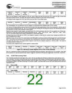
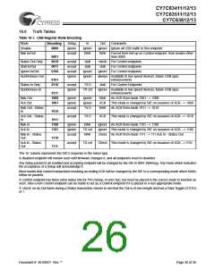
Endpoint 0
Set-up
Received
Endpoint 0
In
Received
Endpoint 0
Out
Received
Acknowledge
Mode
Bit 3
Mode
Bit 2
Mode
Bit 1
Mode
Bit 0
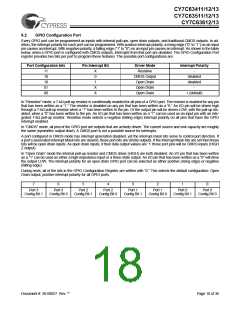
Bits[7:5] in the endpoint 0 mode registers (EPA0) are “sticky” status bits that are set by the SIE to report the type of token that
was most recently received. The sticky bits must be cleared by firmware as part of the USB processing.
The endpoint mode registers for EPA1 and EPA2 do not use bits [7:5] as shown below:
Reserved
Reserved
Reserved
Acknowledge
Mode
Bit 3
Mode
Bit 2
Mode
Bit 1
Mode
Bit 0
The ‘Acknowledge’ bit is set whenever the SIE engages in a transaction that completes with an ‘ACK’ packet.
The ‘set-up’ PID status (bit[7]) is forced HIGH from the start of the data packet phase of the set-up transaction, until the start of
the ACK packet returned by the SIE. The CPU is prevented from clearing this bit during this interval, and subsequently until the
CPU first does an IORD to this endpoint 0 mode register.
Bits[6:0] of the endpoint 0 mode register are locked from CPU IOWR operations only if the SIE has updated one of these bits,
which the SIE does only at the end of a packet transaction (set-up ... Data ... ACK, or Out ... Data ... ACK, or In ... Data ... ACK).
The CPU can unlock these bits by doing a subsequent I/O read of this register.
Firmware must do an IORD after an IOWR to an endpoint 0 register to verify that the contents have changed and that the SIE
has not updated these values.
While the ‘set-up’ bit is set, the CPU cannot write to the DMA buffers at memory locations 0xE0 through 0xE7 and 0xF8 through
0xFF. This prevents an incoming set-up transaction from conflicting with a previous In data buffer filling operation by firmware.
The mode bits (bits [3:0]) in an Endpoint Mode Register control how the endpoint responds to USB bus traffic. The mode bit
encoding is shown in Section 16.0.
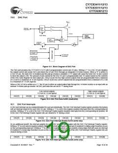
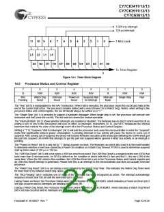
The format of the endpoint Device counter registers is shown below:
Data 0/1
Toggle
Data Valid
Reserved
Reserved
Byte count
Bit 3
Byte count
Bit 2
Byte count
Bit 1
Byte count
Bit 0
Figure 12-2. USB Device Counter Registers 0x11h, 0x13h, 0x15h (read/write)
Bits 0 to 3 indicate the number of data bytes to be transmitted during an IN packet, valid values are 0 to 8 inclusive. Data Valid
bit 6 is used for OUT and set-up tokens only. Data 0/1 Toggle bit 7 selects the DATA packet’s toggle state: 0 for DATA0, 1 for DATA1.
13.0
12-bit Free-running Timer
The 12-bit timer provides two interrupts (128 µs and 1.024 ms) and allows the firmware to directly time events that are up to
4 ms in duration. The lower 8 bits of the timer can be read directly by the firmware. Reading the lower 8 bits latches the upper
4 bits into a temporary register. When the firmware reads the upper 4 bits of the timer, it is actually reading the count stored in
the temporary register. The effect of this logic is to ensure a stable 12-bit timer value can be read, even when the two reads are
separated in time.
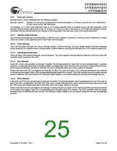
13.1
Timer (LSB)
Timer
Bit 7
Timer
Bit 6
Timer
Bit 5
Timer
Bit 4
Timer
Bit 3
Timer
Bit 2
Timer
Bit 1
Timer
Bit 0
13.2
Timer (MSB)
Reserved
Reserved
Reserved
Reserved
Timer
Bit 11
Timer
Bit 10
Timer
Bit 9
Timer
Bit 8
Document #: 38-08027 Rev. **
Page 22 of 36

 CYPRESS [ CYPRESS ]