CY7C1361B
CY7C1363B
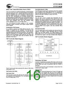
possible to capture all other signals and simply ignore the
value of the CLK captured in the boundary scan register.
Once the data is captured, it is possible to shift out the data by
putting the TAP into the Shift-DR state. This places the
boundary scan register between the TDI and TDO balls.
Note that since the PRELOAD part of the command is not
implemented, putting the TAP to the Update-DR state while
performing a SAMPLE/PRELOAD instruction will have the
same effect as the Pause-DR command.
BYPASS
When the BYPASS instruction is loaded in the instruction
register and the TAP is placed in a Shift-DR state, the bypass
register is placed between the TDI and TDO balls. The
advantage of the BYPASS instruction is that it shortens the
boundary scan path when multiple devices are connected
together on a board.
Reserved
These instructions are not implemented but are reserved for
future use. Do not use these instructions.
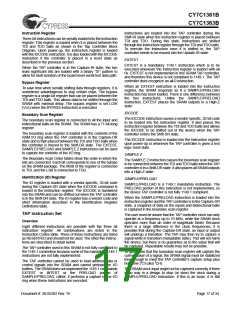
TAP Timing
1
2
3
4
5
6
Test Clock
(TCK)
t
t
t
CYC
TH
TL
t
t
t
t
TMSS
TDIS
TMSH
Test Mode Select
(TMS)
TDIH
Test Data-In
(TDI)
t
TDOV
t
TDOX
Test Data-Out
(TDO)
DON’T CARE
UNDEFINED
TAP AC Switching Characteristics Over the operating Range[9, 10]
Parameter
Clock
tTCYC
tTF
Description
Min.
Max.
Unit
TCK Clock Cycle Time
TCK Clock Frequency
TCK Clock HIGH time
TCK Clock LOW time
50
ns
MHz
ns
20
tTH
tTL
25
25
ns
Output Times
tTDOV TCK Clock LOW to TDO Valid
tTDOX TCK Clock LOW to TDO Invalid
5
ns
ns
0
Setup Times
tTMSS
TMS Set-Up to TCK Clock Rise
TDI Set-Up to TCK Clock Rise
Capture Set-Up to TCK Rise
5
5
5
ns
ns
tTDIS
tCS
Hold Times
tTMSH
tTDIH
tCH
TMS hold after TCK Clock Rise
TDI Hold after Clock Rise
Capture Hold after Clock Rise
5
5
5
ns
ns
ns
Notes:
t
t
9. CS and CH refer to the setup and hold time requirements of latching data from the boundary scan register.
10. Test conditions are specified using the load in TAP AC test Conditions. T. /t = 1ns
R
F
Document #: 38-05302 Rev. *B
Page 18 of 34

 CYPRESS [ CYPRESS ]