PRELIMINARY
CYW43438
21. Interface Timing and AC Characteristics
Note: Values in this data sheet are design goals and are subject to change based on the results of device characterization.
Unless otherwise stated, the specifications in this section apply when the operating conditions are within the limits specified in Table
22 and Table 24. Functional operation outside of these limits is not guaranteed.
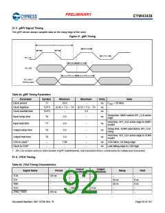
21.1 SDIO Default Mode Timing
SDIO default mode timing is shown by the combination of Figure 35 and Table 42.
Figure 35. SDIO Bus Timing (Default Mode)
fP P
tW L
tW H
S D IO _C LK
tT H L
tT LH
tIH
tIS U
Input
O utput
tO D LY
tO D LY
(m ax)
(m in)
Table 42. SDIO Bus Timing 1 Parameters (Default Mode)
Parameter
Symbol
Minimum
Typical
Maximum
Unit
SDIO CLK (All values are referred to minimum VIH and maximum VIL2)
Frequency—Data Transfer mode
Frequency—Identification mode
Clock low time
fPP
fOD
0
0
–
–
–
–
–
–
25
400
–
MHz
kHz
ns
tWL
tWH
tTLH
tTHL
10
10
–
Clock high time
–
ns
Clock rise time
10
10
ns
Clock fall time
–
ns
Inputs: CMD, DAT (referenced to CLK)
Input setup time
Input hold time
tISU
tIH
5
5
–
–
–
–
ns
ns
Outputs: CMD, DAT (referenced to CLK)
Output delay time—Data Transfer mode
Output delay time—Identification mode
tODLY
tODLY
0
0
–
–
14
50
ns
ns
1. Timing is based on CL 40 pF load on command and data.
2. min(Vih) = 0.7 × VDDIO and max(Vil) = 0.2 × VDDIO.
Document Number: 002-14796 Rev. *K
Page 90 of 101

 CYPRESS [ CYPRESS ]