PRELIMINARY
CYW43438
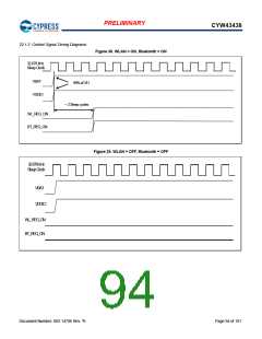
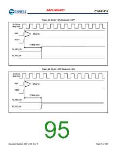
22. Power-Up Sequence and Timing
22.1 Sequencing of Reset and Regulator Control Signals
The CYW43438 has two signals that allow the host to control power consumption by enabling or disabling the Bluetooth, WLAN, and
internal regulator blocks. These signals are described below. Additionally, diagrams are provided to indicate proper sequencing of the
signals for various operational states (see Figure 38 through Figure 41). The timing values indicated are minimum required values;
longer delays are also acceptable.
Note:
■ The WL_REG_ON and BT_REG_ON signals are OR’ed in the CYW43438. The diagrams show both signals going high at the same
time (as would be the case if both REG signals were controlled by a single host GPIO). If two independent host GPIOs are used
(one for WL_REG_ON and one for BT_REG_ON), then only one of the two signals needs to be high to enable the CYW43438
regulators.
■ The reset requirements for the Bluetooth core are also applicable for the FM core. In other words, if FM is to be used, then the
Bluetooth core must be enabled.
■ The CYW43438 has an internal power-on reset (POR) circuit. The device will be held in reset for a maximum of 110 ms after VDDC
and VDDIO have both passed the POR threshold (see Table 24: “Recommended Operating Conditions and DC Characteristics” ).
Wait at least 150 ms after VDDC and VDDIO are available before initiating SDIO accesses.
■ VBAT and VDDIO should not rise faster than 40 µs. VBAT should be up before or at the same time as VDDIO. VDDIO should not
be present first or be held high before VBAT is high.
22.1.1 Description of Control Signals
■ WL_REG_ON: Used by the PMU to power up the WLAN section. It is also OR-gated with the BT_REG_ON input to control the
internal CYW43438 regulators. When this pin is high, the regulators are enabled and the WLAN section is out of reset. When this
pin is low the WLAN section is in reset. If both the BT_REG_ON and WL_REG_ON pins are low, the regulators are disabled.
■ BT_REG_ON: Used by the PMU (OR-gated with WL_REG_ON) to power up the internal CYW43438 regulators. If both the
BT_REG_ON and WL_REG_ON pins are low, the regulators are disabled. When this pin is low and WL_REG_ON is high, the BT
section is in reset.
Note: For both the WL_REG_ON and BT_REG_ON pins, there should be at least a 10 ms time delay between consecutive toggles
(where both signals have been driven low). This is to allow time for the CBUCK regulator to discharge. If this delay is not followed,
then there may be a VDDIO in-rush current on the order of 36 mA during the next PMU cold start.
Document Number: 002-14796 Rev. *K
Page 93 of 101

 CYPRESS [ CYPRESS ]