BCM4330 Preliminary Data Sheet
Power-Up Sequence and Timing
Section 23: Power-Up Sequence and Timing
Sequencing of Reset and Regulator Control Signals
The BCM4330 has three signals that allow the host to control power consumption by enabling or disabling the
Bluetooth, WLAN, and internal regulator blocks. These signals are described below. Additionally, diagrams are
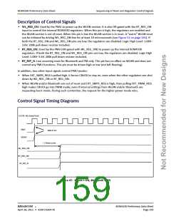
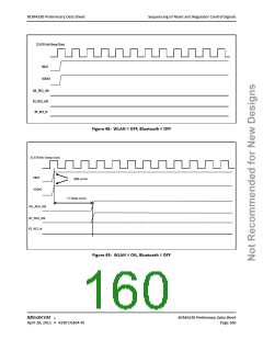
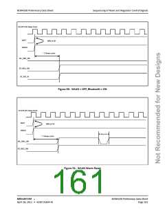
provided to indicate proper sequencing of the signals for various operational states (see Figure 47 on page 159,
Figure 48 on page 160, Figure 49 on page 160 and Figure 50 on page 161). The timing values indicated are the
minimum required values; longer delays are also acceptable.
Note: The WL_REG_ON and BT_REG_ON signals are ORed in the BCM4330. The diagrams show both
signals going high at the same time (as would be the case if both REG signals were controlled by a
single host GPIO). If two independent host GPIOs are used (one for WL_REG_ON and one for
BT_REG_ON), then only one of the two signals needs to be high to enable the BCM4330 regulators.
Also note that the reset requirements for the Bluetooth core are also applicable for the FM core. In other
words, if FM is to be used, then the Bluetooth core must be enabled.
Note: The BCM4330 has an internal power-on reset (POR) circuit. The device will be held in reset for
a maximum of 110 ms after VDDC and VDDIO have both passed the 0.6V threshold. Wait at least 150
ms after VDDC and VDDIO are available before initiating SDIO accesses. The external reset signals are
logically ORed with this POR. So if either the internal POR or one of the external resets is asserted,
the device will be in reset.
If VDDIO goes LOW, all regulators (including bandgap reference) will be powered OFF immediately,
regardless of the status of the WL_REG_ON, BT_REG_ON, and EXT_SMPS_REQ pins.
®
BROADCOM
BCM4330 Preliminary Data Sheet
April 28, 2011 • 4330-DS304-RI
Page 158

 CYPRESS [ CYPRESS ]