BCM4330 Preliminary Data Sheet
Package Information
Section 24: Package Information
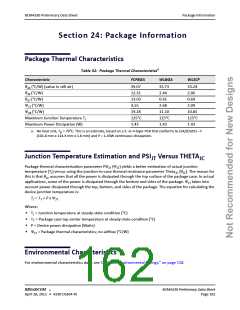
Package Thermal Characteristics
Table 52: Package Thermal Characteristicsa
Characteristic
(°C/W) (value in still air)
FCFBGA
WLBGA
WLSCP
θ
39.07
12.31
13.03
4.55
33.73
2.44
0.61
33.24
2.06
0.69
JA
θ (°C/W)
JB
θ (°C/W)
JC
Ψ (°C/W)
2.68
2.09
JT
Ψ (°C/W)
Maximum Junction Temperature T
Maximum Power Dissipation (W)
19.28
125°C
1.43
11.10
125°C
1.43
10.85
125°C
1.43
JB
J
a. No heat sink, T = 70°C. This is an estimate, based on a 2- or 4-layer PCB that conforms to EIA/JESD51–7
A
(101.6 mm x 114.3 mm x 1.6 mm) and P = 1.43W continuous dissipation.
Junction Temperature Estimation and PSI Versus THETA
JT
JC
Package thermal characterization parameter PSI (Ψ ) yields a better estimation of actual junction
JT
JT
temperature (T ) versus using the junction-to-case thermal resistance parameter Theta (θ ). The reason for
J
JC JC
this is that θ assumes that all the power is dissipated through the top surface of the package case. In actual
JC
applications, some of the power is dissipated through the bottom and sides of the package. Ψ takes into
JT
account power dissipated through the top, bottom, and sides of the package. The equation for calculating the
device junction temperature is:
TJ = TT + P x ΨJT
Where:
• T = Junction temperature at steady-state condition (°C)
J
• T = Package case top center temperature at steady-state condition (°C)
T
• P = Device power dissipation (Watts)
• Ψ = Package thermal characteristics; no airflow (°C/W)
JT
Environmental Characteristics
For environmental characteristics data, see Table 25: “Environmental Ratings,” on page 118.
®
BROADCOM
BCM4330 Preliminary Data Sheet
Page 162
April 28, 2011 • 4330-DS304-RI

 CYPRESS [ CYPRESS ]