BCM4330 Preliminary Data Sheet
SDIO/gSPI Timing
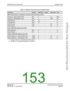
SDIO High-Speed Mode Timing
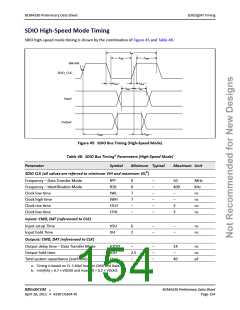
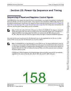
SDIO high-speed mode timing is shown by the combination of Figure 45 and Table 48.
fPP
tWL
tWH
50% VDD
SDIO_CLK
tTHL
tTLH
tIH
tISU
Input
Output
tODLY
tOH
Figure 45: SDIO Bus Timing (High-Speed Mode)
Table 48: SDIO Bus Timinga Parameters (High-Speed Mode)
Symbol Minimum Typical
SDIO CLK (all values are referred to minimum VIH and maximum VILb)
Parameter
Maximum Unit
Frequency – Data Transfer Mode
Frequency – Identification Mode
Clock low time
Clock high time
Clock rise time
fPP
0
0
7
7
–
–
–
–
–
–
–
–
50
400
–
–
3
MHz
kHz
ns
ns
ns
fOD
tWL
tWH
tTLH
tTHL
Clock low time
3
ns
Inputs: CMD, DAT (referenced to CLK)
Input setup Time
Input hold Time
tISU
tIH
6
2
–
–
–
–
ns
ns
Outputs: CMD, DAT (referenced to CLK)
Output delay time – Data Transfer Mode
Output hold time
Total system capacitance (each line)
tODLY
tOH
CL
–
2.5
–
–
–
–
14
–
40
ns
ns
pF
a. Timing is based on CL 40pF load on CMD and Data.
b. min(Vih) = 0.7 × VDDIO and max(Vil) = 0.2 × VDDIO.
®
BROADCOM
BCM4330 Preliminary Data Sheet
April 28, 2011 • 4330-DS304-RI
Page 154

 CYPRESS [ CYPRESS ]