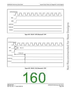
BCM4330 Preliminary Data Sheet
HSIC Interface Specifications
HSIC Interface Specifications
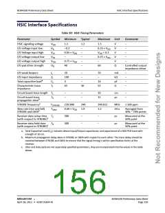
Table 50: HSIC Timing Parameters
Parameter
Symbol Minimum
Typical
Maximum Unit
Comments
HSIC signaling voltage
I/O voltage input low
I/O Voltage input high
I/O voltage output low
I/O voltage output high
I/O pad drive strength
V
V
V
V
V
1.1
1.2
–
–
–
–
1.3
0.35 × V
V
V
V
V
V
Ω
–
–
–
–
–
DD
–0.3
0.65 × V
–
0.75 × V
40
IL
DD
DD
V
+ 0.3
IH
DD
DD
DD
0.25 × V
–
60
OL
OH
O
–
Controlled output
impedance driver
D
I/O weak keepers
I/O input impedance
Total capacitive load
Characteristic trace
impedance
I
Z
C
T
20
100
3
–
–
–
50
70
–
14
55
mA
kΩ
pF
Ω
–
–
–
–
L
I
a
L
45
I
Circuit board trace length
Circuit board trace
T
T
–
–
–
–
10
15
cm
ps
–
–
L
S
b
propagation skew
c
STROBE frequency
F
239.988
0.60 × V
240
1.0
240.012
1.2
MHz
V/ns
± 500 ppm
Averaged from
30% ~ 70% points
Measured at the
50% point
Measured at the
50% point
STROBE
Slew rate (rise and fall)
T
T
T
slew
DD
C
STROBE and DATA
Receiver data setup time
(with respect to STROBE)
300
300
–
–
–
–
ps
ps
s
c
Receiver data hold time
(with respect to STROBE)
b
c
a. Total Capacitive Load (C ), includes device Input/Output capacitance, and capacitance of a 50Ω PCB trace with
L
a length of 10 cm.
b. Maximum propagation delay skew in STROBE or DATA with respect to each other. The trace delay should be
matched between STROBE and DATA to ensure that the signal timing is within specification limits at the
receiver.
c. Jitter and duty cycle are not separately specified parameters, they are incorporated into the values in the table
above.
®
BROADCOM
BCM4330 Preliminary Data Sheet
April 28, 2011 • 4330-DS304-RI
Page 156

 CYPRESS [ CYPRESS ]