CY7C1359A/GVT71256T18
Boundary Scan Order (continued)
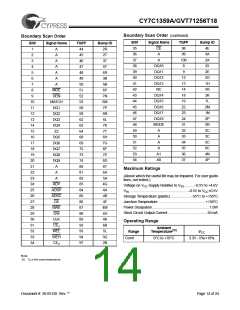
Boundary Scan Order
Bit#
35
36
37
38
39
40
41
42
43
44
45
46
47
48
49
50
51
52
53
54
Signal Name
CE
TQFP
98
99
100
8
Bump ID
4E
Bit#
1
Signal Name
A
TQFP
44
45
46
47
48
49
50
51
52
53
58
59
62
63
64
68
69
72
73
74
80
81
82
83
84
85
86
87
88
89
92
93
94
97
Bump ID
2R
2T
A
3A
2
A
A
2A
3
A
3T
DQ10
DQ11
DQ12
DQ13
NC
ID
4
A
5T
9
2E
5
A
6R
3B
5B
6P
7N
6M
7P
6N
6L
12
13
14
18
19
22
23
24
31
32
33
34
35
36
37
2G
1H
5R
2K
6
A
7
A
8
MOE
DEN
MATCH
DQ1
DQ2
DQ3
DQ4
ZZ
DQ14
DQ15
DQ16
DQ17
DQ18
MODE
A
9
1L
10
11
12
13
14
15
16
17
18
19
20
21
22
23
24
25
26
27
28
29
30
31
32
33
34
2M
1N
2P
3R
2C
3C
5C
6C
4N
4P
7K
7T
A
DQ5
DQ6
DQ7
DQ8
DQ9
A
6H
7G
6F
A
A
A1
7E
6D
6T
A0
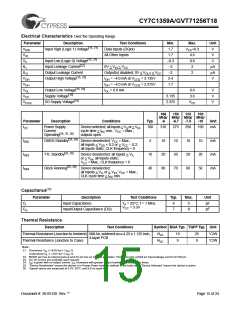
Maximum Ratings
A
6A
5A
4G
4A
4B
4F
(Above which the useful life may be impaired. For user guide-
lines, not tested.)
A
ADV
ADSP
ADSC
OE
Voltage on VCC Supply Relative to VSS..........–0.5V to +4.6V
VIN .......................................................... –0.5V to VCC+0.5V
Storage Temperature (plastic) ................... –55°C to +150°C
Junction Temperature ............................................... +150°C
Power Dissipation.......................................................... 1.0W
Short Circuit Output Current........................................ 50 mA
BWE
GW
CLK
CE2
WEL
WEH
CE2
4M
4H
4K
6B
5L
Operating Range
Ambient
Range
Com’l
Temperature[20]
VCC
3G
2B
0°C to +70°C
3.3V −5%/+10%
Note:
20. TA is the case temperature.
Document #: 38-05120 Rev. **
Page 14 of 24

 CYPRESS [ CYPRESS ]