CY7C1359A/GVT71256T18
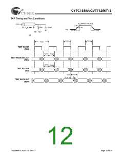
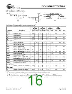
AC Test Loads and Waveforms
ALL INPUT PULSES
+2.5v
1,667
DQ
2.5V
0V
90%
10%
90%
Z = 50
Ω
50Ω
30 pF
Ω
0
10%
DQ
Vt = 1.25V
(a)
≤ 1.8 ns
≤ 1.8 ns
1,538Ω
5 pF
(c)
(b)
(b)
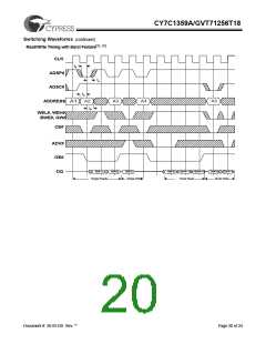
Switching Characteristics Over the Operating Range[27]
-6
-6.7
150 MHz
-7.5
133 MHz
-10
100 MHz
166 MHz
Parameter
Clock
tKC
Description
Min.
Max.
Min.
Max.
Min.
Max.
Min.
Max.
Unit
Clock Cycle Time
6.0
6.7
7.5
8.5
ns
Clock Frequency
Clock HIGH Time
Clock LOW Time
tKF
tKH
2.4
2.4
2.6
2.6
2.8
2.8
3.4
3.4
ns
ns
tKL
Output Times
tKQ
Clock to Output Valid
3.5
3.8
4.0
4.0
ns
ns
tKM
Clock to MATCH Valid
tKQX
Clock to Output Invalid
1.5
1.5
1.5
1.5
tKMX
Clock to MATCH Invalid
tKQLZ
Clock to Output in Low-Z[17, 28, 29]
Clock to Output in High-Z[17, 28, 29]
OE to Output Valid[30]
0
0
0
0
ns
ns
ns
tKQHZ
tOEQ
tMOEM
tOELZ
1.5
6.0
3.5
1.5
6.7
3.5
1.5
7.5
3.8
1.5
8.5
3.8
MOE to MATCH Valid[30]
OE to Output in Low-Z[17, 28, 29]
MOE to MATCH in Low-Z[17, 28, 29]
OE to Output in High-Z[17, 28, 29]
MOE to MATCH in High-Z[17, 28, 29]
0
0
0
0
ns
ns
tMOELZ
tOEHZ
tMOEHZ
Set-up Times
tS
3.5
3.5
3.8
3.8
Address, Controls, and Data In[31]
Address, Controls, and Data In[31]
1.5
0.5
1.5
0.5
1.5
0.5
2.0
0.5
ns
ns
Hold Times
tH
Notes:
27. Test conditions as specified with the output loading as shown in part (a) of AC Test Loads unless otherwise noted.
28. Output loading is specified with CL = 5 pF as in AC Test Loads.
29. At any given temperature and voltage condition, tKQHZ is less than tKQLZ, tOEHZ is less than tOELZ and tMOEHZ is less than tMOELZ
30. OE is a “Don’t Care” after a write cycle begins To prevent bus contention, OE should be negated prior before the start of write cycle.
31. This is a synchronous device. All synchronous inputs must meet specified set-up and hold time, except for “don’t care” as defined in the truth table.
.
Document #: 38-05120 Rev. **
Page 16 of 24

 CYPRESS [ CYPRESS ]