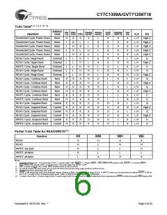
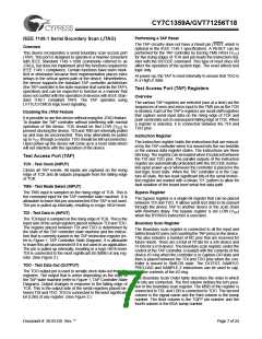
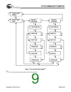
CY7C1359A/GVT71256T18
0
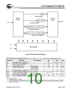
Bypass Register
Selection
Circuitry
Selection
Circuitry
2
1
0
TDO
TDI
Instruction Register
29
Identification Register
31 30
.
.
2
1
1
0
0
.
x
.
.
.
2
Boundary Scan Register [14]
TDI
TDI
TAP Controller
Figure 2. TAP Controller Block Diagram
TAP DC Electrical Characteristics (20°C < Tj < 110°C; VCC = 3.3V –0.2V and +0.3V unless otherwise noted)
Parameter
Description
Test Conditions
Min.
2.0
Max.
VCC + 0.3
0.8
Unit
VIH
VIl
Input High (Logic 1) Voltage[15, 16]
Input Low (Logic 0) Voltage[15, 16]
Input Leakage Current
V
V
–0.3
–5.0
–5.0
ILI
0V < VIN < VCC
5.0
µA
µA
ILO
Output Leakage Current
Output disabled,
0V < VIN < VCCQ
5.0
VOLC
VOHC
VOLT
LVCMOS Output Low Voltage[15, 17] IOLC = 100 µA
LVCMOS Output High Voltage[15, 17] IOHC = 100 µA
0.2
0.4
V
V
V
V
VCC – 0.2
LVTTL Output Low Voltage[15]
LVTTL Output High Voltage[15]
IOLT = 8.0 mA
IOHT = 8.0 mA
VOHT
2.4
Notes:
14. X = 53 for this device.
15. All Voltage referenced to VSS (GND).
16. Overshoot: VIH(AC)<VCC+1.5V for t<tKHKH/2, Undershoot: VIL(AC)<–0.5V for t<tKHKH/2, Power-up: VIH<3.6V and VCC<3.135V and VCCQ<1.4V for t<200 ms.
During normal operation, VCCQ must not exceed VCC. Control input signals (such as GW, ADSC, etc.) may not have pulse widths less than tKHKL (min.).
17. This parameter is sampled.
Document #: 38-05120 Rev. **
Page 10 of 24

 CYPRESS [ CYPRESS ]