Huajing Discrete Devices
R
○
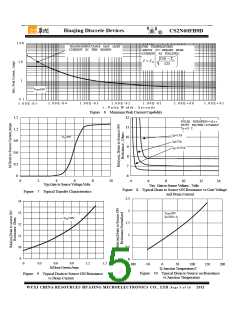
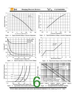
1.2
1.1
1
1.15
VDS=VGS
ID=250μA
1.1
ID=250μA
1.05
1.0
0.9
0.8
0.7
0.6
0.95
0.9
0.85
-100
-50
0
50
100
150
200
-100
-50
0
50
100
Tj,Junction Temperature,C
150
200
Tj,Junction Temperature,C
Figure 12 Typical Breakdown Voltage vs Junction Temperature
Figure 11 Typical Theshold Voltage vs Junction Temperature
250
14
12
VGS=0V , f=1MHz
Ciss=Cgs+Cgd
Coss=Cds+Cgd
Crss=Cgd
200
10
VDS=480V
ID=1.5A
150
8
6
4
2
0
100
50
0
Ciss
Coss
Crss
0
2
4
6
8
10
12
14
0
10
20
30
40
50
Qg,Total gate charge, nc
Vds,Drain to source Voltage,Volts
Figure 13 Typical Capacitance vs Drain to Source Voltage
Figure 14 Typical Gate Charge vs Gate to Source Voltage
1.2
1
10
1
STARTING Tj = 25℃
STARTING Tj = 150℃
0.8
0.6
0.4
0.2
0
+150℃
+25℃
-55℃
0.1
If R=0: tAV=(L* IAS) / (1.38VDSS-VDD
)
If R≠0: tAV=(L/R) In[IAS*R/ (1.38VDSS-VDD)+1]
R equals total Series resistance of Drain circuit
0.01
0.2
0.4
Vsd,Source-Drain to source voltages,volts
Figure 15 Typical Body Diode Transfer Characteristics
0.6
0.8
1
1.2
1.00E-06 1.00E-05 1.00E-04 1.00E-03 1.00E-02 1.00E-01
tav , Time in Avalanche , Seconds
Figure 16 Unclamped Inductive Switching Capability
WUXI CHINA RESOURCES HUAJING MICROELECTRONICS CO., LTD. Page 6 of 10
2011

 CONSONANCE [ Shanghai Consonance Electronics Incorporated ]