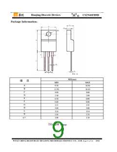
Huajing Discrete Devices
R
○
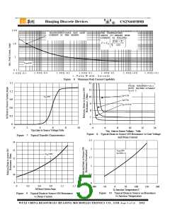
Source-Drain Diode Characteristics
Rating
Symbol
Parameter
Test Conditions
Units
Min.
--
Typ.
Max.
1.5
Continuous Source Current (Body Diode)
Maximum Pulsed Current (Body Diode)
Diode Forward Voltage
IS
--
A
A
ISM
VSD
trr
--
--
6.0
IS=1.5A,VGS=0V
--
--
1.5
V
Reverse Recovery Time
--
250
550
4.4
ns
nC
A
IS=1.5A,Tj = 25°C
Reverse Recovery Charge
Qrr
IRRM
--
dIF/dt=100A/us,
VGS=0V
Reverse Recovery Current
--
Pulse width tp≤380µs,δ≤2%
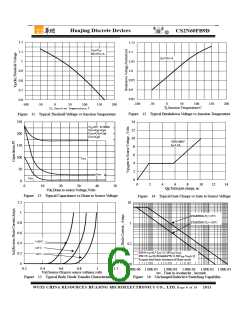
Symbol
Parameter
Typ.
5.21
100
Units
Junction-to-Case
Rθ
℃/W
℃/W
JC
Junction-to-Ambient
Rθ
JA
Gate-source Zener diode
Rating
Symbol
Parameter
Test Conditions
Units
V
Min.
Typ.
Max.
IGS= ±1mA(Open Drain)
VGSO
Gate-source breakdown voltage
20
The built-in back-to-back Zener diodes have specifically been designed to enhance not only the device’s
ESD capability, but also to make them safely absorb possible voltage transients that may occasionally be
applied from gate to source. In this respect the Zener voltage is appropriate to achieve an efficient and
cost-effective intervention to protect the device’s integrity. These integrated Zener diodes thus avoid the
usage of external components.
a1:Repetitive rating; pulse width limited by maximum junction temperature
a2:L=10.0mH, ID=4A, Start TJ=25℃
a3:ISD =1.5A,di/dt ≤100A/us,VDD≤BVDS, Start TJ=25℃
WUXI CHINA RESOURCES HUAJING MICROELECTRONICS CO., LTD. Page 3 of 10
2011

 CONSONANCE [ Shanghai Consonance Electronics Incorporated ]