CX82100 Home Network Processor Data Sheet
9.3.10
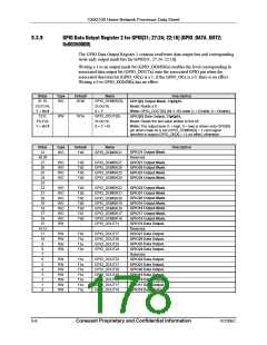
GPIO Data Output Register 3 for GPIO[39:37; 32] (GPIO_DATA_OUT3:
0x003500D4)
The GPIO Data Output Register 3 contains read/write data output bits and corresponding
write-only output mask bits for GPIO[39:32].
Writing a 1 to an output mask bit (GPIO_DOMSKx) enables the level corresponding to
associated data output bit (GPIO_DOUTx) onto the associated GPIO pin when the
associated direction bit (GPIO_OEx) is a 1; if the GPIO_OEx is a 0, there is no effect.
Writing a 0 to GPIO_DOMSKx has no effect.
Note: Voltage levels for GPIO[39:37; 32] pins assigned to special purpose functions
by bits in the GPIO_OPT register are reflected in the GPIO_DATA_IN3
register, however, the GPIO_DATA_OUT3 register bits are not applicable.
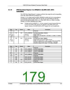
Bit(s)
31:24
Type
Default
Name
Description
Reserved.
23:16;
23≥Y≥16,
Y = Bit #
15:8
7:0;
7≥Y≥0,
Y = Bit #
RO
8’b0
GPIO_DOMSK{X},
39≥X≥32,
GPIO[X] Output Mask, 39≥X≥32.
Read: Reads a 0.
Write: GPIO_DOUT[X] (bit Y-=16) mask (1 = Enable; 0 = Disable).
Reserved.
GPIO[X] Data Output, 39≥X≥32.
Read: Reads the last value written to this bit.
Write: The output level (1 = high, 0 = low) is driven onto GPIO[X]
pin when mask bit is set (GPIO_DOMSK[X] = 1) and signal
direction is output (GPIO_OE[X] = 1); no effect, otherwise.
X = Y+16
RW
8’bx
GPIO_DOUT{X},
39≥X≥32,
X = Y+32
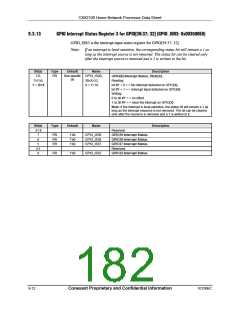
Bit(s)
31:24
23
22
21
20:17
16
15:8
7
6
5
Type
Default
Name
Description
Reserved.
GPIO39 Output Mask.
GPIO38 Output Mask.
GPIO37 Output Mask.
Reserved.
GPIO32 Output Mask.
Reserved.
GPIO39 Data Output.
GPIO38 Data Output.
GPIO37 Data Output.
Reserved.
RO
RO
RO
1’b0
1’b0
1’b1
GPIO_DOMSK39
GPIO_DOMSK38
GPIO_DOMSK37
RO
1’b1
GPIO_DOMSK32
RW
RW
RW
-
-
GPIO_DOUT39
GPIO_DOUT38
GPIO_DOUT37
1’b1
4:1
0
RW
1’b1
GPIO_DOUT32
GPIO32 Data Output.
101306C
Conexant Proprietary and Confidential Information
9-9

 CONEXANT [ CONEXANT SYSTEMS, INC ]