CX82100 Home Network Processor Data Sheet
9.3.4
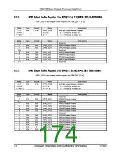
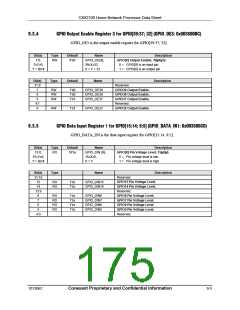
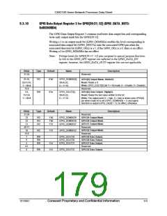
GPIO Output Enable Register 3 for GPIO[39:37; 32] (GPIO_OE3: 0x003500BC)
GPIO_OE3 is the output enable register for GPIO[39:37; 32].
Bit(s)
Type
RW
Default
8’b0
Name
GPIO_OE{X},
39≥X≥32,
Description
GPIO[X] Output Enable, 39≥X≥32.
0 = GPIO[X] is an input pin.
1 = GPIO[X] is an output pin.
7:0;
7≥Y≥0,
Y = Bit #
X = Y + 32
Bit(s)
31:8
7
6
5
4:1
0
Type
Default
Name
Description
Reserved.
RW
RW
RW
1’b0
1’b0
1’b1
GPIO_OE39
GPIO_OE38
GPIO_OE37
GPIO39 Output Enable.
GPIO38 Output Enable.
GPIO37 Output Enable.
Reserved.
RW
1’b1
GPIO_OE32
GPIO32 Output Enable.
9.3.5
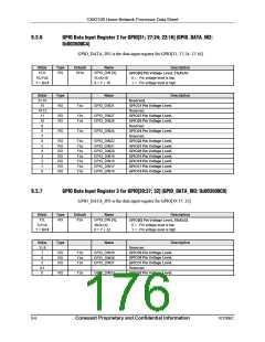
GPIO Data Input Register 1 for GPIO[15:14; 8:5] (GPIO_DATA_IN1: 0x003500C0)
GPIO_DATA_IN1is the data input register for GPIO[15:14; 8:5].
Bit(s)
15:0;
15≥Y≥0,
Y = Bit #
Type
RO
Default
16’bx
Name
GPIO_DIN {X},
15≥X≥0,
Description
GPIO[X] Pin Voltage Level, 15≥X≥0.
0 = Pin voltage level is low.
X = Y
1 = Pin voltage level is high.
Bit(s)
31:16
15
14
13:9
8
7
6
5
4:0
Type
Name
Description
Reserved.
GPIO15 Pin Voltage Level.
GPIO14 Pin Voltage Level.
Reserved.
GPIO8 Pin Voltage Level.
GPIO7 Pin Voltage Level.
GPIO6 Pin Voltage Level.
GPIO5 Pin Voltage Level.
Reserved.
RO
RO
1’bx
1’bx
GPIO_DIN15
GPIO_DIN14
RO
RO
RO
RO
1’bx
1’bx
1’bx
1’bx
GPIO_DIN8
GPIO_DIN7
GPIO_DIN6
GPIO_DIN5
101306C
Conexant Proprietary and Confidential Information
9-5

 CONEXANT [ CONEXANT SYSTEMS, INC ]