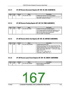
CX82100 Home Network Processor Data Sheet
9
General Purpose Input/Output Interface Description
9.1
GPIO Pin Description
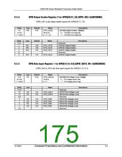
The GPIO pins can be read by reading GPIO_DATA_IN{x} register. They can be driven
as outputs by using GPIO_OE{x} for the pin driver enable, and GPIO_DATA_OUT{x}
for the data output polarity.
Each GPIO[x] pin is controlled individually by GPIO_OE{x} for the input/output
direction. All GPIO pins can serve as external interrupt inputs. These are controlled
through GPIO_ISR{x} and GPIO_IER{x} registers. The polarity and the sensitivity (i.e.,
edge or level) for each GPIO interrupt source can be controlled by programming the
GPIO_IPC{x} and GPIO_ISM{x} registers, respectively.
GPIO[39:37; 32] have alternate functions that can be controlled through the GPIO Option
Register (GPIO_OPT).
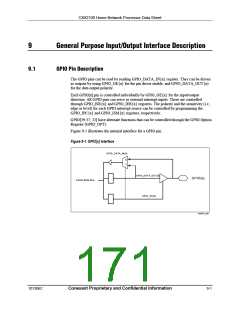
Figure 9-1 illustrates the internal interface for a GPIO pin.
Figure 9-1. GPIO[x] Interface
GPIO_DATA_IN{x}
0
1
GPIO_DATA_OUT{x}
GPIO[x]
Local data bus
GPIO_OE{x}
100545_061
101306C
Conexant Proprietary and Confidential Information
9-1

 CONEXANT [ CONEXANT SYSTEMS, INC ]