CX82100 Home Network Processor Data Sheet
9.3
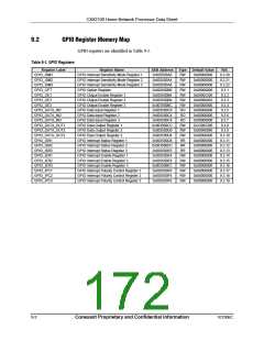
GPIO Registers
GPIO register bits are described in this section.
9.3.1
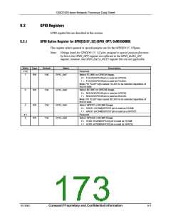
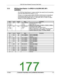
GPIO Option Register for GPIO[39:37; 32] (GPIO_OPT: 0x003500B0)
This register selects general or special purpose use for the GPIO[39:37; 32] pins.
Note: Voltage levels for GPIO[39:37; 32] pins assigned to special purpose functions
by bits in the GPIO_OPT register are reflected in the GPIO_DATA_IN3
register, however, the GPIO_DATA_OUT3 register bits are not applicable.
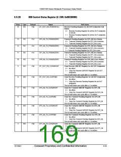
Bit(s)
31:8
7
Type
Default
Name
GPIO_Sel7
Description
Reserved.
RW
1’b0
Select FCLKIO or GPIO39 Usage.
0 = FCLKIO/GPIO39 pin is used as GPIO39.
1 = FCLKIO/GPIO39 pin is used as FCLKIO.
Note: Pin PLLBP high causes FCLKIO to be selected regardless of
this bit state.
6
5
RW
1’b0
GPIO_Sel6
Select BCLKIO or GPIO38 Usage.
0 = BCLKIO/GPIO38 pin is used as GPIO38.
1 = BCLKIO/GPIO38 pin is used as BCLKIO.
Note: Pin PLLBP high causes BCLKIO to be selected regardless of
this bit state.
RW
RW
1’b0
1’b0
GPIO_Sel5
GPIO_Sel0
Select GPIO37 or HCS4# Usage.
0 = HAD31 (HCS4#)/GPIO37 pin is used as HCS4#.
1 = HAD31 (HCS4#)/GPIO37 pin is used as a GPIO37.
Reserved.
4:1
0
Select GPIO32 or HCS0# Usage.
0 = HC00 (HCS0#)/GPIO32 pin is used as HCS0#.
1 = HC00 (HCS0#)/GPIO32 pin is used as GPIO32.
101306C
Conexant Proprietary and Confidential Information
9-3

 CONEXANT [ CONEXANT SYSTEMS, INC ]