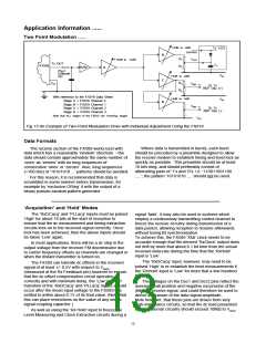
Application Information ......
Two Point Modulation ......
+3dB to -3dB
Tx VCO
CONTROL
B
R1
R2
VVCO
+14dB to -14dB
Tx OUT
C1
FX589
Buffer
A
Fig.2
External
RC
VSS
+3dB to -3dB
C
D
VSS
R3
R4
VREF
(+)
To Tx
REF Osc (+)
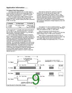
With reference to the FX019 Data Sheet
Stage A = FX019 Channel 4
Stage B = FX019 Channel 1
Stage C = FX019 Channel 2
Stage D = FX019 Channel 3
+3dB to -3dB
VSS
VREF
(-)
To Tx
REF Osc (-)
Note that ALL stages of the FX019 are ’Inverting’ stages
VSS
Fig.13 An Example of Two-Point Modulation Drive with Individual Adjustment Using the FX019
Data Formats
Where data is transmitted in bursts, each burst
should be preceded by a preamble designed to allow
the receive modem to establish timing and level lock as
quickly as possible. This preamble should be at least
16 bits long, and should preferably consist of
The receive section of the FX589 works best with
data which has a reasonably ‘random’ structure --the
data should contain approximately the same number of
‘ones’ as ‘zeroes’ with no long sequences of
consecutive ‘ones’ or ‘zeroes’. Also, long sequences
(>100 bits) of ‘10101010 ...’ patterns should be avoided.
alternating pairs of ‘1’s and ‘0’s i.e. ‘110011001100
.....’; the pattern ‘10101010 ....’ should not be used.
For this reason, it is recommended that data is
scrambled in some manner before transmission, for
example by ‘exclusive-ORing’ it with the output of a
binary pseudo-random pattern generator.
‘Acquisition’ and ‘Hold’ Modes
The ‘RxDCacq’ and ‘PLLacq’ inputs must be pulsed
‘High’ for about 16 bits at the start of reception to
ensure that the dc measurement and timing extraction
circuits lock-on to the received signal correctly. Once
lock has been achieved, then the above inputs should
be taken ‘Low’ again.
signal ‘fade’, it may also be used in systems which
employ a continuously transmitting control channel to
freeze the receive circuitry during transmission of a
data packet, allowing reception to resume afterwards
without losing bit synchronisation.
To achieve this, the FX589 ‘Xtal’ clock needs to be
accurate enough that the derived ‘RxClock’ output does
not drift by more that about 0.1 bit time from the actual
received data-rate during the time that the ‘RxHold’
input is ‘Low’.
In most applications, there will be a dc step in the
output voltage from the receiver FM discriminator due
to carrier frequency offsets as channels are changed or
when the distant transmitter is turned on.
The ‘RxDCacq’ input, however, may need to be
pulsed ‘High’ to re-establish the level measurements if
the ‘RxHold’ input is ‘Low’ for more that a few hundred
bit-times.
The FX589 can tolerate dc offsets in the received
signal of at least +/- 0.5V with respect to VBIAS
,
(measured at the Rx Feedback pin) however to ensure
that the dc offset compensation circuit operates
correctly and with minimum delay, the ‘Low’ to ‘High’
transition of the ‘RxDCacq’ and ‘PLLacq’ inputs should
occur after the mean input voltage to the FX589 has
settled to within about 0.1V of its final value. (Note that
this can place restrictions on the value of any series
signal coupling capacitor.)
The voltages on the Doc1 and Doc2 pins reflect the
average peak positive and negative excursions of the
(filtered) receive signal, and could therefore be used to
derive a measure of the data signal amplitude.
Note however, that these pins are driven from very
high-impedance circuits, so that the dc load presented
by any external circuitry should exceed 10MΩ to VBIAS
.
As well as using the ‘Rx Hold’ input to freeze the
Level Measuring and Clock Extraction circuits during a
13

 CMLMICRO [ CML MICROCIRCUITS ]