Application Information ......
10-1
10-2
10-3
Tx and Rx DC coupled
Tx 5Hz, Rx DC coupled
Tx 5Hz, Rx 10Hz
10-4
Tx 5Hz, Rx 30Hz
Tx 5Hz, Rx 100Hz
10-5
4
5
6
7
8
9
10
11
12
13
S/N (dB) (noise in 8kHz bandwidth)
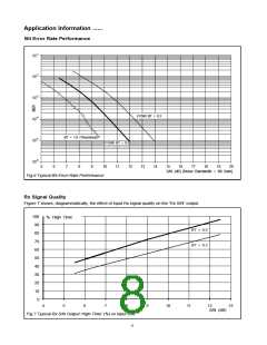
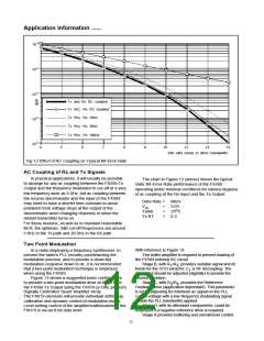
Fig.12 Effect of AC Coupling on Typical Bit-Error Rate
AC Coupling of Rx and Tx Signals
In practical applications, it will usually be possible
to arrange for any ac coupling between the FX589 Tx
Output and the frequency modulator to cut-off at a very
low frequency such as 5.0Hz, but ac coupling between
the receive discriminator and the input of the FX589
may need to have a shorter time-constant to avoid
problems from voltage steps at the output of the
discriminator when changing channels or when the
distant transmitter turns on.
The chart in Figure 12 (above) shows the typical
static Bit-Error-Rate performance of the FX589
operating under nominal conditions for various degrees
of ac coupling at the Rx Input and the Tx Output:
Data Rate = 8kb/s
VDD
Tamb
Tx BT
=
=
=
5.0V
25 C
0.3
o
For these reasons, as well as to maintain reasonable
BER, the optimum -3dB cut-off frequencies are around
5.0Hz in the Tx path and 20.0Hz in the Rx path.
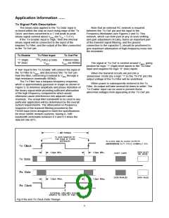
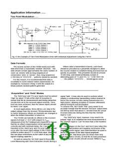
Two Point Modulation
With reference to Figure 13:
The buffer amplifier is required to prevent loading of
the FX589 external RC circuit.
In a radio employing a frequency synthesiser, to
prevent the radio's PLL circuitry counteracting the
modulation process, and to provide a clean flat
modulation response down to dc, it is recommended
that a two-point modulation technique is employed
when using the FX589.
Figure 13 shows a suggested basic configuration
to provide a two-point modulation drive at 8kb/s from
the FX589 Tx Output using the FX019 (a CML product)
Digitally Controlled ‘Quad’ Amplifier Array.
Stage B, with R /R , provides suitable signal and dc
1
2
levels for the VCO varactor; C is RF decoupling. The
1
drive level should be adjusted (digitally) to provide the
desired deviation.
Stage C, with R /R , provides the Reference
3
4
Oscillator drive (application dependant). This parameter
is set by adjusting for minimum ac signal on the PLL
control voltage with a low-frequency modulating signal
(inside the PLL bandwidth) applied.
The FX019 elements will provide individual setting-up,
calibration and dynamic control of modulation levels.
Level setting control of the amplifiers/attenuators of the
FX019 is via an 8-bit data word.
Stage D, with its attendant components, could be
employed if a negative reference drive is required.
Stage A provides buffering and overall level control.
12

 CMLMICRO [ CML MICROCIRCUITS ]