GMSK Packet Data Modem and RF Transceiver
CMX990
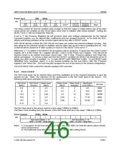
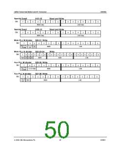
Power Up 2
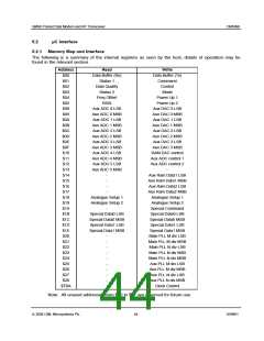
$05
Write
7
6
5
4
3
2
1
0
Bit:
AUX
DAC3
AUX
DAC2
AUX
DAC1
AUX
DAC0
LNA ON
(External)
Preserve
Registers
RESET
Vbias
The Vbias control bit must be enabled early enough so that the output is stable before any of the other
circuit blocks are enabled as this circuit takes some time to stabilise after being enabled. Setting the
RESET bit to '1' will not change the Vbias bit.
If set to '1' the Preserve Registers bit will preserve most user settings programmed via the Special
Command register, e.g. Rx channel filter coefficients and non assigned memory. In Rx mode the AGC,
offsets and timing estimates of the received signal will be lost after a RESET event.
LNA ON bit directly controls the LNA ON pin and does not control any internal analogue circuitry. Any
time delay for the external circuitry to stabilise must be taken into account when controlling this bit. This
control bit will be cleared to '0' after a power on reset or if the RESET bit is set to '1'.
Whenever a '1' is written to the RESET bit all registers will be cleared to '0' apart from the Clock Control
register, bit 5 of the Power Up 1 register and bits 1 and 0 of the Power Up 2 register. This will put all
internal circuits in an inactive and power saved state. The 'V Reg', 'Preserve registers' and 'Vbias' bits
will be unchanged. To ensure a clean exit from the RESET condition the RESET bit should be set to '0'
before any other circuitry is enabled. i.e. To enter RESET write '000010xx' to $05. To exit RESET write
'000000xx' then 'xxxx0xxx', where 'x' is the desired condition for the Aux DACs, LNA ON, 'Preserve
registers' and 'Vbias' bits. The host may then program the rest of the device to the desired configuration.
The AUX DAC0-3 bits control the relevant auxiliary D2A converter.
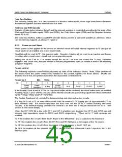
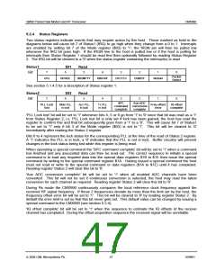
5.2.3 Clock Control
The Ref Clock input can be divided down and then multiplied up to the required frequency to give the
desired bit rate. Note: The reference for the synthesizers is the Ref Clock input to the device. The
following table gives examples for common bit rates:
Ref clock
(MHz)
Ref Clock
Division
Base clock
(MHz)
Base clock Base clock
Baseband
clock (MHz)
Bit rate
(MHz)
multiplier
4.8
12
2
5
5
7
8
9
2.4
2.4
2.88
2.4
2.4
2.4
2.4
4
9.6
4000
8000
16000
4800
9600
2.4
2.4
8
16
4
19.2
14.4
16.8
19.2
21.6
38.4
2.88
2.88
11.52
23.04
8
The Ref clock input to the device must be in the range 3.8MHz to 24MHz.
The Base Clock resulting from the division of the Ref Clock must be in the range 1.9MHz to 3.0MHz.
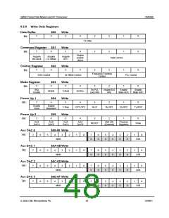
Clock Control
$TBA Write
7
6
5
4
3
2
1
0
Bit:
Base clock multiplier, 2 - 16
Ref Clock division, 2 - 16
(0000 = x16, 0001 = Illegal state)
(0000 = /16, 0001 = Illegal state)
Notes: 1) To program '16' the host should load '0000', the value '0001' for both the above values should
not be programmed.
2) The baseband clock will not be available for TBAms after exiting Reset.
ã 2004 CML Microsystems Plc
46
D/990/1

 CMLMICRO [ CML MICROCIRCUITS ]