GMSK Packet Data Modem and RF Transceiver
CMX990
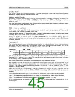
Data Bus Buffers
The circuitry driving the D0-7 pins consists of 8 internal bidirectional 3-state logic level buffers between
the internal registers and the external data bus lines.
Address and R/W Decode
Transfer of data bytes between the µC and the internal registers is controlled according to the state of the
Write and Read Enable inputs (WRN and RDN), the Chip Select input (CSN) and the Register Address
inputs A0 to A5.
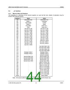
The Data Bus Buffers, Address and R/W Decode blocks provide a byte-wide parallel µC interface, which
can be memory-mapped, as shown in Figure 2.
5.2.2 Power-on and Reset
When power is first applied to the device an internal circuit will reset internal registers to '0' and put all
circuit blocks in an inactive and power saved state.
Read bits will be reset to '0' - the inactive state. Counters / states will be reset to an inactive and known
condition after a reset event - which can occur asynchronously.
Setting the RESET bit to '1' is similar except the RESET bit does not control the 'V Reg', 'Preserve
registers' and 'Vbias' bits, they will remain at the last programmed state, as shown in bold in the following
2 register diagrams.
Power control
The following registers control individual power-up state of the indicated blocks. Note: Other sections of
the device have the power control bits included in the control registers for those blocks. Blocks are
disabled and in the zero power state when the associated control bit is '0'.
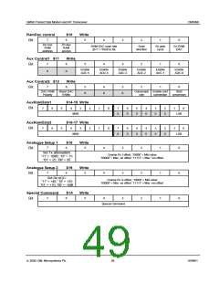
Power Up 1
$04
Write
7
6
5
4
3
2
1
0
Bit:
Enable
Clock
Enable
Baseband
Enable
OP1 OP2
V Reg
Rx IF
Rx RF1
Rx RF2
Tx RFIF
If the Enable Clock is set to '0' the on chip clock buffer will be disabled, the clock buffer must be enabled
if setting RESET (bit 3 of $05) or if any of the internal circuits are powered up apart from those controlled
by the 'V Reg', 'Vbias' and 'OP1 OP2' bits.
The Enable Baseband bit controls the data packeting and clock extraction circuits.
If V Reg bit is set to '0' an internal circuit will hold the nominal 2.5V supply pins at approximately 2V for
data retention only. For normal operation the host must set this bit to '1' before enabling any other
circuitry. If an external supply provides the nominal 2.5V then the V Reg bit should be set to '0'. See
section 4.5 for more details.
When the OP1 OP2 bit is low both OP 1 and OP 2 amplifiers are disabled the OP1T and OP2T pins will
become high impedance inputs to ADC2 and ADC3 respectively. When set to ‘1’ both op-amps are
enabled.
Rx IF bit enables the circuitry from the IF IN pin to the differential I and Q outputs to the baseband.
Rx RF1 bit enables the circuitry from the RF IN A and RF IN B pins to the output of the 1st mixers.
Rx RF2 bit enables the circuitry from the output of the 1st mixers to the IF OUT pin.
Tx RFIF bit enables all the transmit RF and IF circuits from the differential I and Q inputs to the Tx RF
interface pins.
ã 2004 CML Microsystems Plc
45
D/990/1

 CMLMICRO [ CML MICROCIRCUITS ]