GMSK Packet Data Modem and RF Transceiver
CMX990
The Fast setting allows the modem to respond quickly without µC intervention - although at the
cost of reduced Bit Error Rate versus Signal to Noise performance.
Note that the AFC measuring system requires ‘00’ and ‘11’ bit pairs to be received at
reasonably frequent intervals. The AFC tracking will eventually fail if ‘1’ or ‘0’ is transmitted
continuously.
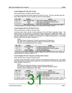
Control Register B1, B0: PLL Control
These two bits have no effect in transmit mode.
In receive mode, they set the ‘normal’ bandwidth of the Rx clock extraction Phase Locked Loop
circuit. This setting will be temporarily overridden by the Acquire Bit Clock command (bit 7 of
Command register) which will go through a sequence depending if a frame sync is being
searched for (SFH or SFS task is started within 14 bits):
Frame sync search:
No frame sync search:
16 bits of wide setting
30 bits of medium setting
Revert to normal setting
Wide setting until Frame Sync is detected
30 bits of medium setting
Revert to normal setting
B1 B0
PLL Bandwidth
Hold
Suggested use
0
0
1
1
0
1
0
1
Signal fades
Narrow
Medium
Wide
< ± 20ppm bit rate error systems
Wide bit rate error or long preamble acquisition
Quick acquisition
The ‘hold’ setting is intended for use during signal fades, otherwise the minimum bandwidth
consistent with the transmit and receive modem bit rate tolerances should be chosen.
The wide and medium bandwidth settings allow the modem to respond rapidly to fresh
messages and recover rapidly after a fade without µC intervention - although at the cost of
reduced Bit Error Rate versus Signal to Noise performance.
Note that the clock extraction circuits work by detecting the timing of edges, i.e. a change from
‘0’ to ‘1’ or ‘1’ to ‘0’. The clock extraction will eventually fail if ‘1’ or ‘0’ is transmitted
continuously
ã 2004 CML Microsystems Plc
32
D/990/1

 CMLMICRO [ CML MICROCIRCUITS ]