GMSK Packet Data Modem and RF Transceiver
CMX990
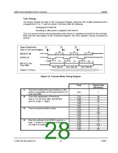
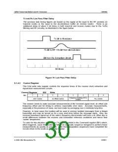
Tx and Rx Low Pass Filter Delay
The previous task timing figures are based on the signal at the input to the RF sections (in
transmit mode) or the input to the de-interleave buffer (in receive mode). There is an
additional delay of about 2 bit times in both transmit and receive modes due to the Tx/Rx
filtering and RF circuitry, as illustrated in the figure below.
Figure 16 Low Pass Filter Delay
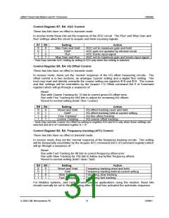
5.1.4.3 Control Register
This 8-bit write only register controls the response times of the receive clock extraction and
signal level measurement circuits.
Control Register
$02
Write
7
6
5
4
3
2
1
0
Bit:
Frequency tracking (AFC)
Control
AGC Control
IQ Offset Control
PLL Control
The modem needs to make accurate measurements of the received signal level, dc offset and
frequency offset and bit timing to achieve reasonable error rates. Accurate measurements,
especially in the presence of noise, are best made by averaging over a relatively long time.
However, in most cases the modem will be used to receive isolated messages from a distant
transmitter and may be turned on for a very short time before the message starts. Also, the
received baseband signal out of the radio's frequency discriminator will have a dc offset due to
small differences between the receiver and transmitter reference oscillators and hence their
‘carrier’ frequencies.
To cater for this situation acquire bits 7 to 5 are provided in the Command register ($01) which,
when triggered, cause the modem to follow an automatic sequence designed to perform these
measurements as quickly as possible. After these acquisition sequences have completed the
circuits return to the mode as set in this register.
ã 2004 CML Microsystems Plc
30
D/990/1

 CMLMICRO [ CML MICROCIRCUITS ]