Marine VHF Audio and Signalling Processor
CMX885
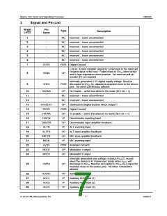
48-pin
L4/Q3
Pin
Name
Type
Description
30
31
ADC4
AVDD
IP
Auxiliary ADC input (4)
Positive 3.3V supply rail for the analogue on-chip circuits.
Levels and thresholds within the device are proportional to
this voltage. This pin should be decoupled to AVSS by
capacitors mounted close to the device pins.
PWR
32
33
34
35
36
37
DAC1
DAC2
AVSS
DAC3
DAC4
DVSS
OP
OP
Auxiliary DAC output 1/RAMDAC
Auxiliary DAC output 2
PWR Analogue Ground
OP
OP
Auxiliary DAC output 3
Auxiliary DAC output 4
PWR Digital Ground
Internally generated 2.5V supply voltage. Must be decoupled
38
VDEC
PWR to DVSS by capacitors mounted close to the device pins. No
other connections allowed.
Input to the oscillator inverter from the Xtal circuit or external
clock source.
39
40
XTAL/CLK
XTALN
IP
OP
The output of the on-chip Xtal oscillator inverter
The 3.3V positive supply rail for the digital on-chip circuits.
41
DVDD
PWR This pin should be decoupled to DVss by capacitors mounted
close to the device pins
42
43
CDATA
RDATA
IP
TS OP
NC
C-BUS: Serial data input from the µC
C-BUS: A 3-state C-BUS serial data output to the µC. This
output is high impedance when not sending data to the µC.
44
45
46
47
-
Reserved – do not connect this pin
DVSS
PWR Digital Ground
SCLK
IP
C-BUS: The C-BUS serial clock input from the µC
SYSCLK2
OP
Synthesised Digital System Clock Output 2
C-BUS: The C-BUS chip select input from the µC - there is
no internal pullup on this input
48
CSN
IP
~
On this device, the central metal pad (which is exposed on
Q3 packages only) may be electrically unconnected or,
alternatively, may be connected to Analogue Ground (AVss).
No other electrical connections are permitted.
EXPOSED
SUBSTRATE
METAL PAD
Notes: IP
=
=
=
=
=
=
Input (+ PU/PD = internal pullup/pulldown resistor)
Output
Bidirectional
3-state Output
Power Connection
No Connection - should NOT be connected to any signal
OP
BI
TS OP
PWR
NC
© 2010 CML Microsystems Plc
8
D/885/3

 CMLMICRO [ CML MICROCIRCUITS ]