Marine VHF Audio and Signalling Processor
CMX885
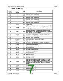
3
Signal and Pin List
48-pin
L4/Q3
Pin
Name
Type
Description
reserved – leave unconnected
1
2
3
4
5
6
7
-
NC
NC
NC
NC
NC
NC
-
reserved – leave unconnected
reserved – leave unconnected
reserved – leave unconnected
reserved – leave unconnected
reserved – leave unconnected
-
-
-
-
DVSS
PWR Digital Ground
C-BUS: A 'wire-ORable' output for connection to the Interrupt
Request input of the host. Pulled down to DVSS when active
and is high impedance when inactive. An external pull-up
resistor (R1) is required.
8
9
IRQN
OP
Internally generated 2.5V digital supply voltage. Must be
PWR decoupled to DVSS by capacitors mounted close to the device
pins. No other connections allowed.
VDEC
10
11
12
13
14
15
16
17
18
19
20
21
22
23
24
RXENA
-
OP
NC
NC
OP
Rx Enable – active low when in Rx mode ($C1:b0 = 1)
reserved – leave unconnected
-
reserved – leave unconnected
SYSCLK1
DVSS
TXENA
DISCN
DISCFB
ALTN
ALTFB
MICFB
MICN
AVSS
MOD1
MOD2
Synthesised Digital System Clock Output 1
PWR Digital Ground
OP
IP
Tx Enable – active low when in Tx mode ($C1:b1 = 1)
Discriminator inverting input
Discriminator input amplifier feedback
ALT inverting input
OP
IP
OP
OP
IP
ALT input amplifier feedback
MIC input amplifier feedback
MIC inverting input
PWR Analogue Ground
OP
OP
Modulator 1 output
Modulator 2 output
Internally generated bias voltage of about AVDD/2, except
when the device is in ‘Powersave’ mode when VBIAS will
discharge to AVSS. Must be decoupled to AVSS by a capacitor
mounted close to the device pins. No other connections
allowed.
25
VBIAS
OP
26
27
28
29
AUDIO
ADC1
ADC2
ADC3
OP
IP
Audio output
Auxiliary ADC input (1)
Auxiliary ADC input (2)
Auxiliary ADC input (3)
IP
IP
© 2010 CML Microsystems Plc
7
D/885/3

 CMLMICRO [ CML MICROCIRCUITS ]