Marine VHF Audio and Signalling Processor
CMX885
1.1
History
Version Changes
Date
3
20/12/201
0
• Clarified operation of Data End bit (b7) for DSC Rx mode in section 8.1.22.
• Clarified the need for observing C-BUS latency when writing multiple C-BUS
commands in section 7.3.
• Minor typographical corrections in table of section 8.1.27, P4.10 and P4.11
values in section 8.2.5.
2
8/4/2010
• Changed "Modem Control" to "Modem Cofiguration" register
• Bit references changed to "$C1:b12" style, for consistency
• Changed name of $C1:b2 to "Modem Enable" and $C!:b4 to "Modem Source"
• Deleted other references to "processing" in the description of $C1 register bits
• Deleted the reference to "clearing the En_DSC bit" at the end of section 7.7.1
• Xtal frequency tolerance in section 9.1.4 changed from 100ppm to 30ppm, to
meet DSC specifications.
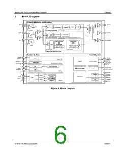
• Corrected DAC3 to DAC4 in figure 1.
• +1dB and 3dB limits apply to all Rx and Tx responses (figures 6 to 10).
Wording changed accordingly in section 7.5.
• "write" added to description of Audio Tone register ($CD) in section 7.6.
• Reference in $C1 to bits 11-9 should read 11-8 in section 7.6.
• Program Block registers P3.2 to P3.6 should read P3.2 - P3.7 in section 7.11.1.
• GPIO RXENA and TXENA signals - nomenclature standardised in section 7.12.
• Hyperlink added for $C1 in section 8.1.
• Correction of $C0 b6 to "BIAS Block Enable" in section 8.1.17.
• Merge table rows for $CE b9 in section 8.1.28.
• Removed references to MSK: these should be DSC in sections 7.7.1 and 7.7.2.
• Clarification of Status register bit 3, Modem Control register bits 3-8 and bit 11,
Interrupt Mask register bits 3 and 5.
• Footnotes in Parametric Specifications harmonised with table references.
• Minor typographical corrections.
• This document created – based on 7041FI-1.x documentation
1
18/9/2009
© 2010 CML Microsystems Plc
5
D/885/3

 CMLMICRO [ CML MICROCIRCUITS ]