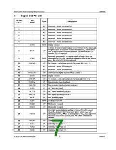
Marine VHF Audio and Signalling Processor
CMX885
Notes:
1. X1 can be a crystal or an external clock generator; this will depend on the application. The tracks
between the crystal and the device pins should be as short as possible to achieve maximum stability
and best start up performance. By default, a 3.6864MHz clock is selected, other values could be
used if the various internal clock dividers are set to appropriate values.
2. R5 should be selected to provide the desired dc gain (assuming C11 is not present) of the DISCN
input, as follows:
⏐GAINDISCN⏐ = 100kΩ / R5
The gain should be such that the resultant output at the DISCFB pin is within the input signal range
specified in 7.13.2.
3. R7 should be selected to provide the desired dc gain (assuming C13 is not present) of the ALTN
input as follows:
⏐GAINALTN⏐ = 100kΩ / R7
The gain should be such that the resultant output at the ALTFB pin is within the input signal range
specified in 7.13.
4. R9 should be selected to provide the desired dc gain (assuming C15 is not present) of the MICN
input as follows:
⏐GAINMICN⏐ = 100kΩ / R9
The gain should be such that the resultant output at the MICFB pin is within the input signal range
specified in 7.13.1. For optimum performance with low signal microphones, an additional external
gain stage may be required.
5. C11, C13 and C15 should be selected to maintain the lower frequency roll-off of the MICN, ALTN
and DISCN inputs as follows:
C11 ≥ 100nF × ⏐GAINDISCN
C13 ≥ 100nF × ⏐GAINALTN
C15 ≥ 30nF × ⏐GAINMICN
⏐
⏐
⏐
6. ALTN and ALTFB connections allow the user to have an additional signal input. Component
connections and values are as for the respective DISCN and MICN networks. If this input is not
required, the ALTN pin should be connected to AVss.
7. C5 (AUDIO output) should be increased to 1.0µF if frequencies below 300Hz need to be used on
this pin.
8. A single 10µF electrolytic capacitor (C24, fitted as shown) may be used for smoothing the power
supply to both VDEC pins, providing they are connected together on the pcb with an adequate width
power supply trace. Alternatively, separate smoothing capacitors should be connected to each
VDEC pin. High frequency decoupling capacitors (C3 and C23) must always be fitted as close as
possible to both VDEC pins.
© 2010 CML Microsystems Plc
11
D/885/3

 CMLMICRO [ CML MICROCIRCUITS ]