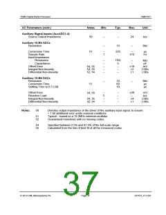
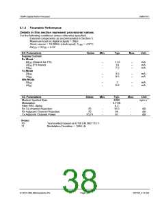
TDMA Digital Radio Processor
CMX7161
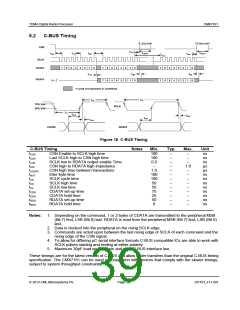
8.3
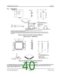
Packaging
TYP.
DIM.
MAX.
MIN.
9.00 BSC
A
B
C
F
*
*
9.00 BSC
0.90
1.00
7.80
7.80
0.05
0.30
0.80
7.00
7.00
G
0.00
0.18
0.20
0.30
0
H
J
K
L
L1
0.25
0.40
0.50
0.15
P
T
0.50
0.20
NOTE :
A & B are reference data and do
not include mold deflash or protrusions.
*
All dimensions in mm
Angles are in degrees
Exposed
Metal Pad
Index Area 1
Index Area 2
Dot
Dot
Chamfer
Index Area 1 is located directly above Index Area 2
Depending on the method of lead termination at the edge of the package, pull back (L1) may be present.
L minus L1 to be equal to, or greater than 0.3mm
The underside of the package has an exposed metal pad which should ideally be soldered to the pcb to enhance the thermal
conductivity and mechanical strength of the package fixing. Where advised, an electrical connection to this metal pad may also
be required
Figure 19 Mechanical Outline of 64-lead VQFN (Q1)
Order as part no. CMX7161Q1
Figure 20 Mechanical Outline of 64-pin LQFP (L9)
Order as part no. CMX7161L9
As package dimensions may change after publication of this datasheet, it is recommended that you check
for the latest Packaging Information from the Design Support/Package Information page of the CML
website: [www.cmlmicro.com].
2013 CML Microsystems Plc
Page 40
D/7161_FI-1.0/4

 CMLMICRO [ CML MICROCIRCUITS ]