TDMA Digital Radio Processor
CMX7161
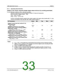
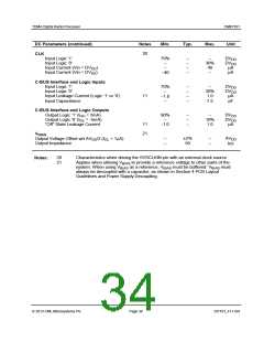
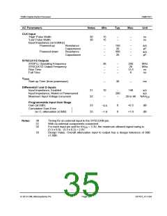
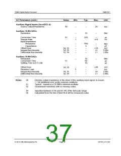
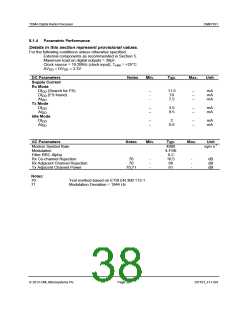
8.2
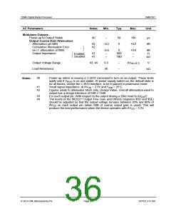
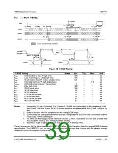
C-BUS Timing
Figure 18 C-BUS Timing
Notes
CSN Enable to SCLK high time
Last SCLK high to CSN high time
SCLK low to RDATA output enable Time
CSN high to RDATA high impedance
CSN high time between transactions
Inter-byte time
C-BUS Timing
Min.
100
100
0.0
–
1.0
100
100
50
50
75
25
50
Typ.
–
–
–
–
–
–
–
–
–
–
–
–
Max.
–
–
–
1.0
–
–
–
–
–
Unit
tCSE
tCSH
tLOZ
tHIZ
ns
ns
ns
µs
µs
ns
ns
ns
ns
ns
ns
ns
ns
tCSOFF
tNXT
tCK
SCLK cycle time
tCH
SCLK high time
tCL
SCLK low time
tCDS
tCDH
tRDS
tRDH
CDATA set-up time
CDATA hold time
RDATA set-up time
RDATA hold time
–
–
–
–
0
–
Notes: 1. Depending on the command, 1 or 2 bytes of CDATA are transmitted to the peripheral MSB
(Bit 7) first, LSB (Bit 0) last. RDATA is read from the peripheral MSB (Bit 7) first, LSB (Bit 0)
last.
2. Data is clocked into the peripheral on the rising SCLK edge.
3. Commands are acted upon between the last rising edge of SCLK of each command and the
rising edge of the CSN signal.
4. To allow for differing µC serial interface formats C-BUS compatible ICs are able to work with
SCLK pulses starting and ending at either polarity.
5. Maximum 30pF load on IRQN pin and each C-BUS interface line.
These timings are for the latest version of C-BUS and allow faster transfers than the original C-BUS timing
specification. The CMX7161 can be used in conjunction with devices that comply with the slower timings,
subject to system throughput constraints.
2013 CML Microsystems Plc
Page 39
D/7161_FI-1.0/4

 CMLMICRO [ CML MICROCIRCUITS ]