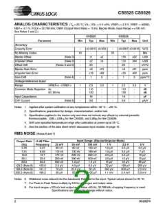
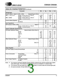
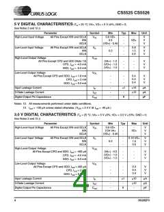
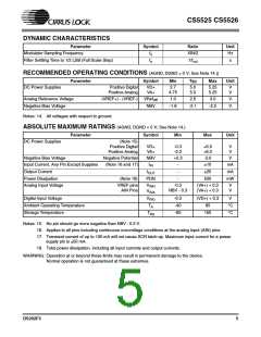
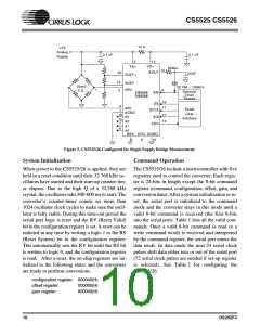
CS5525 CS5526
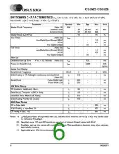
SWITCHING CHARACTERISTICS (T = 25 °C; VA+ = 5 V 5%; VD+ = 3.0 V 10% or 5 V 5%;
A
Input Levels: Logic 0 = 0 V, Logic 1 = VD+; C = 50 pF.))
L
Parameter
Symbol
Min
Typ
Max
Unit
kHz
%
Master Clock Frequency
(Note 19)
Internal Clock
External Clock
XIN
30
30
32.768
32.768
36
100
Master Clock Duty Cycle
Rise Times
40
-
60
(Note 20)
Any Digital Input Except SCLK
SCLK
t
rise
-
-
-
-
-
50
1.0
100
-
µs
µs
ns
Any Digital Output
Fall Times
(Note 20)
Any Digital Input Except SCLK
SCLK
t
fall
-
-
-
-
-
50
1.0
100
-
µs
µs
ns
Any Digital Output
Start-up
Oscillator Start-up Time
XTAL = 32.768 kHz (Note 21)
t
-
-
500
-
-
ms
ost
Power-on Reset Period
t
1003
XIN
por
cycles
Serial Port Timing
Serial Clock Frequency
SCLK
0
-
-
2
-
MHz
ns
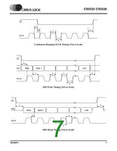
SCLK Falling to CS Falling for continuous running SCLK
(Note 22)
Pulse Width High
Pulse Width Low
t
100
0
Serial Clock
t
t
250
250
-
-
-
-
ns
ns
1
2
SDI Write Timing
CS Enable to Valid Latch Clock
t
t
t
t
50
50
-
-
-
-
-
-
-
-
ns
ns
ns
ns
3
4
5
6
Data Set-up Time prior to SCLK rising
Data Hold Time After SCLK Rising
SCLK Falling Prior to CS Disable
100
100
SDO Read Timing
CS to Data Valid
t
t
t
-
-
-
-
-
-
150
150
150
ns
ns
ns
7
8
9
SCLK Falling to New Data Bit
CS Rising to SDO Hi-Z
Notes: 19. Device parameters are specified with a 32.768 kHz clock; however, clocks up to 100 kHz can be used
for increased throughput.
20. Specified using 10% and 90% points on waveform of interest. Output loaded with 50 pF.
21. Oscillator start-up time varies with crystal parameters. This specification does not apply when using an
external clock source.
22. Applicable when SCLK is continuously running.
6
DS202F3

 CIRRUS [ CIRRUS LOGIC ]