CS49300 Family DSP
12. PIN DESCRIPTIONS
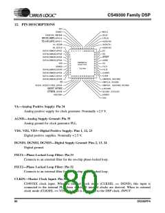
VD1
DGND1
MCLK
SCLK
AUDATA3, XMT958
WR,DS,EMWR,GPIO10
RD,R/W,EMOE,GPIO11
A1, SCDIN
LRCLK
AUDATA0
AUDATA1
A0, SCCLK
AUDATA2
DATA7,EMAD7,GPIO7
DATA6,EMAD6,GPIO6
DATA5,EMAD5,GPIO5
DATA4,EMAD4,GPIO4
VD2
DC
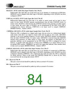
6
5
4
3
2
1
44 43 42 41 40
39
7
8
9
DD
38
37
36
35
34
33
32
31
30
29
RESET
10
11
12
13
14
15
16
17
AGND
CS493XX-CL
44-pin PLCC
VA
DGND2
FILT1
Top View
DATA3,EMAD3,GPIO3
DATA2,EMAD2,GPIO2
DATA1,EMAD1,GPIO1
DATA0,EMAD0,GPIO0
CS
FILT2
CLKSEL
18 19 20 21 22 23 24 25 26 27 28
CLKIN
CMPREQ, LRCLKN2
CMPCLK, SCLKN2
CMPDAT, SDATAN2, RCV958
LRCLKN1
SCDIO, SCDOUT,PSEL,GPIO9
ABOOT, INTREQ
EXTMEM, GPIO8
SDATAN1
SCLKN1, STCCLK2
DGND3
VD3
VA—Analog Positive Supply: Pin 34
Analog positive supply for clock generator. Nominally +2.5 V.
AGND—Analog Supply Ground: Pin 35
Analog ground for clock generator PLL.
VD1, VD2, VD3—Digital Positive Supply: Pins 1, 12, 23
Digital positive supplies. Nominally +2.5 V.
DGND1, DGND2, DGND3—Digital Supply Ground: Pins 2, 13, 24
Digital ground.
FILT1—Phase-Locked Loop Filter: Pin 33
Connects to an external filter for the on-chip phase-locked loop.
FILT2—Phase Locked Loop Filter: Pin 32
Connects to an external filter for the on-chip phase-locked loop.
CLKIN—Master Clock Input: Pin 30
CS493XX clock input. When in internal clock mode (CLKSEL == DGND), this input is
connected to the internal PLL from which all internal clocks are derived. When in external
clock mode (CLKSEL == VD), this input is connected to the DSP clock. INPUT
80
DS339PP4

 CIRRUS [ CIRRUS LOGIC ]