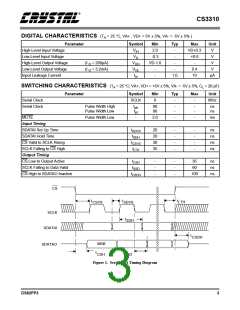
CS3310
In single device operation, volume control data is
loaded into the 16-bit shift register by holding the
CS pin low for sixteen SCLK pulses and then
volume control changes. The gain/attenuation
changes of the CS3310 occur at zero crossings to
eliminate glitches during level transitions. The zero
latched on the rising edge of CS. The previous con- crossing for the left channel is the voltage potential
tents of the shift-register are shifted through the
register and out SDATAO during the process.
at the AGNDL pin; the voltage potential at the
AGNDR pin defines the right channel zero cross-
ing.
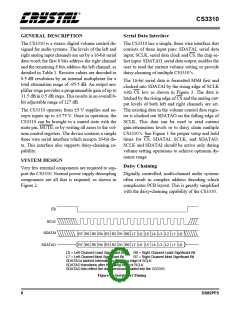
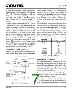
Multi-channel operation can be implemented as
shown in Figure 4 by connecting the SDATAO of A volume control change occurs after chip select
device #1 to the SDATAI pin of device #2. In this
manner multiple CS3310s can be loaded from a
latches the data in the volume control data register
and two zero crossings are detected. If two zero
single serial data line without complex addressing crossings are not detected within 18 ms of the
schemes. Volume control data is loaded by holding change in CS, the new volume setting is imple-
CS low for 16 x N SCLK pulses, where N is the
number of devices in the chain. The 16 bits clocked
mented. The zero crossing enable pin, ZCEN, en-
ables or disables the zero crossing detection
into device #1 on SCLK pulses 1-16 are clocked function as well as the 18 ms time-out circuit.
into device #2 on SCLK pulses 17-32. The
Input Code
CS3310s are simultaneously updated on the rising
edge of CS following 16 x N SCLK pulses. Notice
that a 47 kohm resistor is required to terminate
SDATAI, as shown in Figure 4, due to the high im-
pedance state of SDATAO when CS is high.
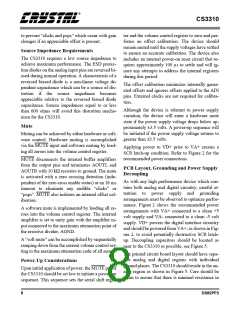
(Left or Right Channel) Gain or Attenuation (dB)
11111111
11111110
•
+31.5
+31.0
•
•
•
11000000
•
00000010
00000001
00000000
0
Changing the Analog Output Level
•
-95.0
-95.5
Care has been taken to ensure that there are no au-
dible artifacts in the analog output signal during
Software Mute
Table 1. Input Code Definition
3
CONTROLLER
6
Analog Inputs and Outputs
SDATAI
SCLK
CS
2
16
9
AINL
AINR
The maximum input level is limited by the com-
mon-mode voltage capabilities of the internal op-
amp. Signals approaching the analog supply volt-
ages may be applied to the AIN pins if the internal
attenuator limits the output signal to within 1.25
volts of the analog supply rails.
AUDIO
SIGNAL
CS3310
#1
14
11
AOUTL
AOUTR
SDATAO
7
47 k
3
6
2
SDATAI
SCLK
CS
The outputs are capable of driving 600 Ω loads to
within 1.25 volts of the analog supply rails and are
short circuit protected to 20 mA.
16
9
AINL
AINR
AUDIO
SIGNAL
CS3310
#2
14
11
AOUTL
AOUTR
As with any adjustable gain stage the affects of a
DC offset at the input must be considered. Capaci-
tively coupling the analog inputs may be required
SDATAO
7
Figure 4. Daisy Chaining Diagram
DS82PP3
7

 CIRRUS [ CIRRUS LOGIC ]