CAT25C11/03/05/09/17
and the WPEN bit) and the block protected sections in
the memory array when the chip is hardware write
protected. Only the sections of the memory array that
are not block protected can be written. Hardware write
protection is disabled when either WP pin is high or the
WPEN bit is zero.
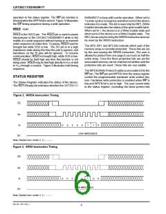
After the correct read instruction and address are sent,
the data stored in the memory at the selected address is
shifted out on the SO pin. The data stored in the memory
atthenextaddresscanbereadsequentiallybycontinuing
to provide clock pulses. The internal address pointer is
automatically incremented to the next higher address
after each byte of data is shifted out. When the highest
address is reached, the address counter rolls over to
0000hallowingthereadcycletobecontinuedindefinitely.
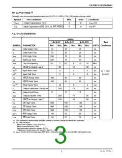
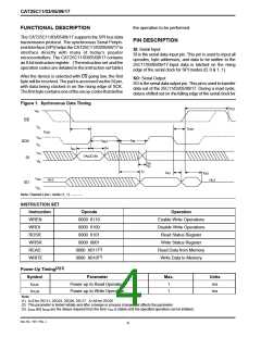
DEVICE OPERATION
Write Enable and Disable
The read operation is terminated by pulling the CS high.
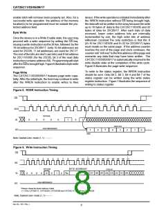
Read sequece is illustrated in Figure 4. Reading status
register is illustrated in Figure 5. To read the status
register, RDSR instruction should be sent. The contents
of the status register are shifted out on the SO line. If a
non-volatile write is in progress, the RDSR instruction
returns a high on SO. When the non-volatile write cycle
is completed, the status register data is read out.
The CAT25C11/03/05/09/17 contains a write enable
latch. This latch must be set before any write operation.
The device powers up in a write disable state when Vcc
is applied. WREN instruction will enable writes (set the
latch) to the device. WRDI instruction will disable writes
(reset the latch) to the device. Disabling writes will
protect the device against inadvertent writes.
READ Sequence
WRITE Sequence
The part is selected by pulling CS low. The 8-bit read
instructionistransmittedtotheCAT25C11/03/05/09/17,
followed by the 16-bit address for 25C09/17 (only 10-bit
addresses are used for 25C09, 11-bit addresses are
used for 25C17. The rest of the bits are don't care bits)
and 8-bit address for 25C11/03/05 (for the 25C05, bit 3
of the read data instruction contains address A8).
The CAT25C11/03/05/09/17 powers up in a Write Dis-
able state. Prior to any write instructions, the WREN
instruction must be sent to CAT25C11/03/05/09/17.
The device goes into Write enable state by pulling the
CS low and then clocking the WREN instruction into
CAT25C11/03/05/09/17. The CS must be brought high
Figure 4. Read Instruction Timing
CS
*
*
0
1
2
3
4
5
6
7
8
9
10
20 21 22 23 24 25 26 27 28 29 30
SK
OPCODE
BYTE ADDRESS*
A
N
A
0
SI
0
0
0
0
X*
0
1
1
DATA OUT
HIGH IMPEDANCE
SO
7
6
5
4
3
2
1
0
MSB
*Please check the Byte Address Table.
*X = 0 for CAT25C11, CAT25C03, CAT25C09 and CAT25C17; X = A8 for CAT25C05.
Note: Dashed Line= mode (1, 1) – – – –
Doc. No. 1017, Rev. J
7

 CATALYST [ CATALYST SEMICONDUCTOR ]