CAT25C11/03/05/09/17
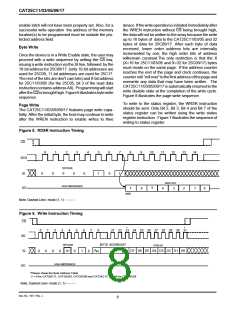
DESIGN CONSIDERATIONS
The CAT25C11/03/05/09/17 powers up in a write dis-
able state and in a low power standby mode. A WREN
instruction must be issued to perform any writes to the
device after power up. Also,on power up CS should be
brought low to enter a ready state and receive an
instruction. After a successful byte/page write or status
register write the CAT25C11/03/05/09/17 goes into a
writedisablemode. CSmustbesethighaftertheproper
number of clock cycles to start an internal write cycle.
Access to the array during an internal write cycle is
ignored and programming is continued. On power up,
SO is in a high impedance. If an invalid op code is
received, no data will be shifted into the CAT25C11/03/
05/09/17, and the serial output pin (SO) will remain in a
high impedance state until the falling edge of CS is
detected again.
Whenpoweringdown,thesupplyshouldbetakendown
to 0V, so that the CAT25C11/03/05/09/17 will be reset
when power is ramped back up. If this is not possible,
then, following a brown-out episode, the CAT25C11/
03/05/09/17 can be reset by refreshing the contents of
the Status Register (See Application Note AN10).
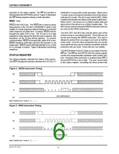
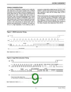
Figure 7. WRSR Instruction Timing
CS
0
1
2
3
4
5
6
7
1
8
9
6
10
5
11
4
12
13
2
14
1
15
0
SCK
OPCODE
DATA IN
SI
0
0
0
0
0
0
0
7
3
MSB
HIGH IMPEDANCE
SO
Note: Dashed Line= mode (1, 1) – – – –
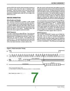
Figure 8. Page Write Instruction Timing
CS
24+(N-1)x8-1..24+(N-1)x8 24+Nx8-1
0
1
2
3
4
5
6
7
8
21 22 23
32-39
24-31
SK
SI
DATA IN
Data Data
Byte 2 Byte 3
BYTE ADDRESS*
A
OPCODE
Data
Byte 1
Data Byte N
A
0
0
0
0
X*
0
1
0
N
0
0
7..1
HIGH IMPEDANCE
SO
*Please check the Byte Address Table.
*X = 0 for CAT25C11, CAT25C03, CAT25C09 and CAT25C17; X = A8 for CAT25C05
Note: Dashed Line= mode (1, 1) – – – –
Doc. No. 1017, Rev. J
9

 CATALYST [ CATALYST SEMICONDUCTOR ]