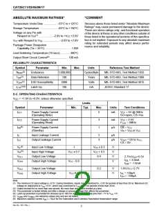
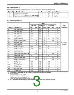
CAT25C11/03/05/09/17
operation to the status register. The WP pin function is
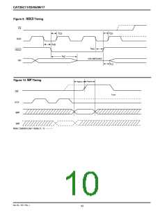
blockedwhentheWPENbitissetto0.Figure10illustrates
the WP timing sequence during a write operation.
03/05/09/17 is busy with a write operation. When set to
1awritecycleisinprogressandwhensetto0thedevice
indicates it is ready. This bit is read only the WEL (Write
Enable) bit indicates the status of the write enable latch.
When set to 1, the device is in a Write Enable state and
when set to 0 the device is in a Write Disable state. The
WELbitcanonlybesetbytheWRENinstructionandcan
be reset by the WRDI instruction.
HOLD: Hold
HOLD is the HOLD pin. The HOLD pin is used to pause
transmission to the CAT25C11/03/05/09/17 while in the
middle of a serial sequence without having to re-transmit
entire sequence at a later time. To pause, HOLD must be
brought low while SCK is low. The SO pin is in a high
impedance state during the time the part is paused, and
transitions on the SI pins will be ignored. To resume
communication, HOLD is brought high, while SCK is low.
HOLD should be held high any time this function is not
being used. HOLD may be tied high directly to VCC or tied
to VCC through a resistor. Figure 9 illustrates hold timing
sequence.
The BP0, BP1 and BP2 bits indicate which part of the
memory array is currently protected. These bits are set
by the user issuing the WRSR instruction. The user is
allowed to protect from one page to as much as half the
entire array. Once the three protection bits are set the
associated memory can be read but not written until the
protection bits are reset. These bits are non volatile.
TheWPEN(WriteProtectEnable)isanenablebitforthe
WP pin. The WP pin and WPEN bit in the status register
control the programmable hardware write protect fea-
ture. Hardware write protection is enabled when WP is
low and WPEN bit is set to high. The user cannot write
to the status register, (including the block protect bits
STATUS REGISTER
The Status Register indicates the status of the device.
The RDY (Ready) bit indicates whether the CAT25C11/
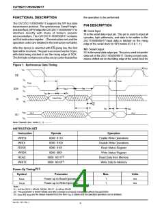
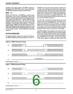
Figure 2. WREN Instruction Timing
CS
SK
1
1
0
SI
0
0
0
0
0
HIGH IMPEDANCE
SO
Note: Dashed Line= mode (1, 1) – – – –
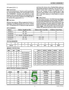
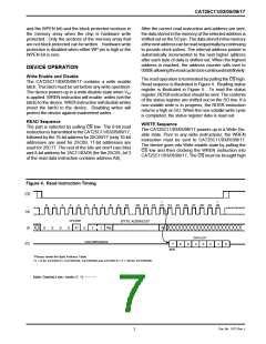
Figure 3. WRDI Instruction Timing
CS
SK
SI
1
0
0
0
0
0
0
0
HIGH IMPEDANCE
SO
Note: Dashed Line= mode (1, 1) – – – –
Doc. No. 1017, Rev. J
6

 CATALYST [ CATALYST SEMICONDUCTOR ]