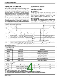
CAT25C11/03/05/09/17
enable latch will not have been properly set. Also, for a
successful write operation the address of the memory
location(s) to be programmed must be outside the pro-
tected address field.
device.Ifthewriteoperationisinitiatedimmediatelyafter
the WREN instruction without CS being brought high,
the data will not be written to the array because the write
up to 16 bytes of data to the CAT25C11/03/05 and 32
bytes of data for 25C09/17. After each byte of data
received, lower order address bits are internally
incremented by one; the high order bits of address
willremain constant.The only restriction is that the X
(X=16 for 25C11/03/05 and X=32 for 25C09/17) bytes
must reside on the same page. If the address counter
reaches the end of the page and clock continues, the
counter will “rollover”tothefirstaddressofthepageand
overwrite any data that may have been written. The
CAT25C11/03/05/09/17 is automatically returned to the
write disable state at the completion of the write cycle.
Figure 8 illustrates the page write sequence.
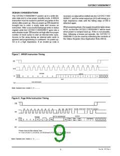
Byte Write
Once the device is in a Write Enable state, the user may
proceed with a write sequence by setting the CS low,
issuing a write instruction via the SI line, followed by the
16-bit address for 25C09/17. (only 10-bit addresses are
used for 25C09, 11-bit addresses are used for 25C17.
The rest of the bits are don't care bits) and 8-bit address
for 25C11/03/05 (for the 25C05, bit 3 of the read data
instructioncontainsaddressA8). Programmingwillstart
aftertheCSisbroughthigh.Figure6illustratesbytewrite
sequence.
To write to the status register, the WRSR instruction
should be sent. Only Bit 2, Bit 3, Bit 4 and Bit 7 of the
status register can be written using the write status
register instruction. Figure 7 illustrates the sequence of
writing to status register.
Page Write
The CAT25C11/03/05/09/17 features page write capa-
bility. After the initial byte, the host may continue to write
after the WREN instruction to enable writes to thee
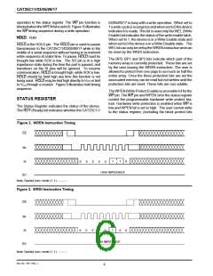
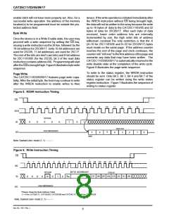
Figure 5. RDSR Instruction Timing
CS
0
1
2
3
4
5
1
6
0
7
1
8
9
10
11
12
13
14
SCK
OPCODE
0
0
0
0
0
SI
DATA OUT
HIGH IMPEDANCE
SO
5
7
6
4
3
2
1
0
MSB
Note: Dashed Line= mode (1, 1) – – – –
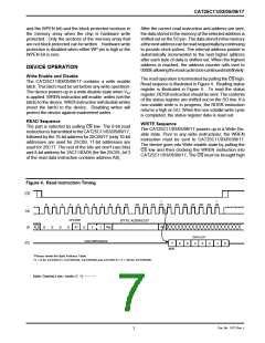
Figure 6. Write Instruction Timing
CS
*
*
0
1
2
3
4
5
6
7
8
21 22 23 24 25 26 27 28 29 30 31
SK
SI
OPCODE
BYTE ADDRESS*
A
DATA IN
A
N
D7 D6 D5 D4 D3 D2 D1 D0
0
0
0
0
0
X*
0
1
0
HIGH IMPEDANCE
SO
*Please check the Byte Address Table
X = 0 for CAT25C11, CAT25C03, CAT25C09 and CAT25C17; X = A8 for CAT25C05
Note: Dashed Line= mode (1, 1) – – – –
Doc. No. 1017, Rev. J
8

 CATALYST [ CATALYST SEMICONDUCTOR ]