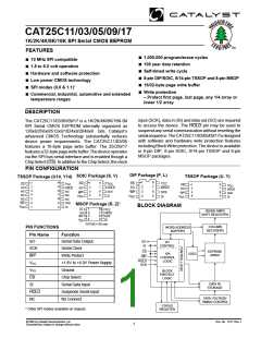
CAT25C11/03/05/09/17
the operation to be performed.
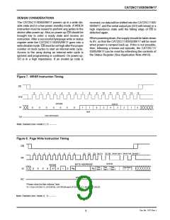
FUNCTIONAL DESCRIPTION
The CAT25C11/03/05/09/17 supports the SPI bus data
transmission protocol. The synchronous Serial Periph-
eral Interface (SPI) helps the CAT25C11/03/05/09/17 to
interface directly with many of today’s popular
microcontrollers. The CAT25C11/03/05/09/17 contains
an8-bitinstructionregister. (Theinstructionset andthe
operation codes are detailed in the instruction set table)
PIN DESCRIPTION
SI: Serial Input
SI is the serial data input pin. This pin is used to input all
opcodes, byte addresses, and data to be written to the
25C11/03/05/09/17.Input data is latched on the rising
edge of the serial clock for SPI modes (0, 0 & 1, 1).
After the device is selected with CS going low, the first
byte will be received. The part is accessed via the SI pin,
with data being clocked in on the rising edge of SCK.
Thefirstbytecontainsoneofthesixop-codesthatdefine
SO: Serial Output
SO is the serial data output pin. This pin is used to transfer
data out of the 25C11/03/05/09/17. During a read cycle,
data is shifted out on the falling edge of the serial clock for
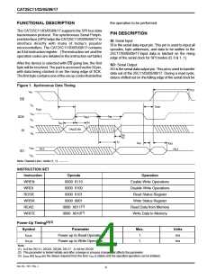
Figure 1. Sychronous Data Timing
t
CS
VIH
CS
VIL
t
CSH
t
CSS
VIH
VIL
t
t
WL
SCK
SI
WH
t
t
H
SU
VIH
VALID IN
V
IL
t
RI
FI
t
t
V
t
t
HO
DIS
VOH
VOL
HI-Z
HI-Z
SO
Note: Dashed Line= mode (1, 1) – – – –
INSTRUCTION SET
Instruction
Opcode
Operation
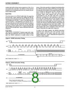
WREN
WRDI
0000 0110
0000 0100
0000 0101
0000 0001
Enable Write Operations
Disable Write Operations
Read Status Register
Write Status Register
Read Data from Memory
Write Data to Memory
RDSR
WRSR
READ
WRITE
(1)
0000 X011
0000 X010
(1)
(2)(3)
Power-Up Timing
Symbol
Parameter
Max.
Units
ms
tPUR
Power-up to Read Operation
Power-up to Write Operation
1
1
tPUW
ms
Note:
(1) X=0 for 25C11, 25C03, 25C09, 25C17. X=A8 for 25C05
(2) This parameter is tested initially and after a design or process change that affects the parameter.
(3) t
and t
are the delays required from the time V is stable until the specified operation can be initiated.
PUR
PUW
CC
Doc. No. 1017, Rev. J
4

 CATALYST [ CATALYST SEMICONDUCTOR ]