PRODUCT SPECIFICATION
TMC3503
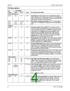
Pin Descriptions (continued)
Pin Number
Pin
Name
LQFP
PLCC
Value
Pin Function Description
R
REF
36
42
590 Ω
Current-setting Resistor. The full-scale output current of each
D/A converter is determined by the value of the resistor
connected between R
and GND. The nominal value for
REF
R
is found from:
REF
REF
R
= 9.1 (V )
/I
REF FS
where I is the full-scale (white) output current (amps) from the
FS
D/A converter (without sync). Sync is 0.4 I
.
FS
D/A full-scale (white) current may also be calculated from:
I
= V /R
FS
FS
L
Where V is the white voltage level and R is the total resistive
FS
L
load (ohms) on each D/A converter. V is the blank to full-scale
FS
voltage.
COMP
34
40
0.1 µF
Compensation Capacitor. A 0.1 µF ceramic capacitor must be
connected between COMP and V
circuitry.
to stabilize internal bias
DD
Power, Ground
12, 30, 31 17, 34–36
V
DD
+5 V
0.0V
Power Supply.
Ground.
GND
1, 14, 15,
27, 28, 38,
39, 48
29–32
NC
13, 24, 25,
37
—
—
No Connect
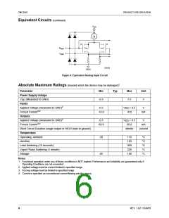
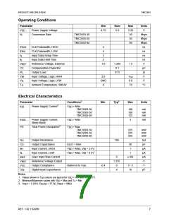
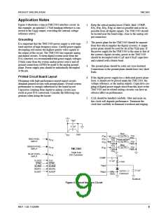
Equivalent Circuits
V
DD
V
DD
p
Digital
Input
n
p
V
DD
n
OUT
GND
GND
27014D
27013B
Figure 2. Equivalent Digital Input Circuit Figure 3. Equivalent Analog Output Circuit
REV. 1.02 11/24/99
5

 CADEKA [ CADEKA MICROCIRCUITS LLC. ]