PRODUCT SPECIFICATION
TMC3503
Application Notes
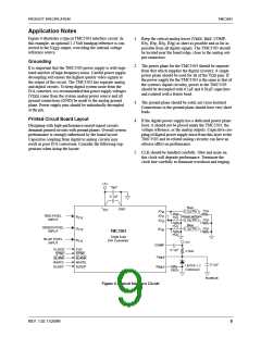
Figure 4 illustrates a typical TMC3503 interface circuit. In
this example, an optional 1.2 Volt bandgap reference is con-
1. Keep the critical analog traces (V , COMP,
, I
IO , IO , IO , IO ) as short as possible and as far as
REF REF
S
R
G
B
nected to the V
reference source.
output, overriding the internal voltage
possible from all digital signals. The TMC3503 should
be located near the board edge, close to the analog out-
put connectors.
REF
Grounding
2. The power plane for the TMC3503 should be separate
from that which supplies the digital circuitry. A single
It is important that the TMC3503 power supply is well-regu-
lated and free of high-frequency noise. Careful power supply
decoupling will ensure the highest quality video signals at
the output of the circuit. The TMC3503 has separate analog
and digital circuits. To keep digital system noise from the
D/A converter, it is recommended that power supply voltages
power plane should be used for all of the V
pins. If
DD
the power supply for the TMC3503 is the same as that of
the system's digital circuitry, power to the TMC3503
should be decoupled with 0.1µF and 0.01µF capacitors
and isolated with a ferrite bead.
(V ) come from the system analog power source and all
DD
ground connections (GND) be made to the analog ground
plane. Power supply pins should be individually decoupled
at the pin.
3. The ground plane should be solid, not cross-hatched.
Connections to the ground plane should have very short
leads.
Printed Circuit Board Layout
4. If the digital power supply has a dedicated power plane
layer, it should not be placed under the TMC3503, the
voltage reference, or the analog outputs. Capacitive cou-
pling of digital power supply noise from this layer to the
TMC3503 and its related analog circuitry can have an
adverse effect on performance.
Designing with high-performance mixed-signal circuits
demands printed circuits with ground planes. Overall system
performance is strongly influenced by the board layout.
Capacitive coupling from digital to analog circuits may
result in poor D/A conversion. Consider the following sug-
gestions when doing the layout:
5. CLK should be handled carefully. Jitter and noise on
this clock will degrade performance. Terminate the
clock line carefully to eliminate overshoot and ringing.
+5V
10µF
0.1µF
Red
O
V
GND
DD
Z
=75Ω
75Ω
75Ω
75Ω
IO
IO
IO
R
S
G
RED PIXEL
INPUT
Green w/Sync
R
75Ω
75Ω
75Ω
7-0
Z
=75Ω
O
Blue
GREEN PIXEL
INPUT
Z
=75Ω
G
B
IO
O
7-0
B
TMC3503
Triple 8-bit
BLUE PIXEL
INPUT
D/A Converter
7-0
+5V
COMP
CLOCK
SYNC
BLANK
WHITE
SLEEP
CLK
0.1µF
590Ω
3.3kΩ
SYNC
BLANK
WHITE
SLEEP
V
R
REF
0.1µF
LM185-1.2
(Optional)
REF
65-3503-05
Figure 4. Typical Interface Circuit
REV. 1.02 11/24/99
9

 CADEKA [ CADEKA MICROCIRCUITS LLC. ]