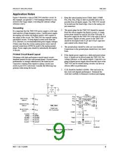
TMC3503
PRODUCT SPECIFICATION
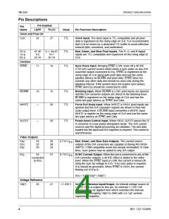
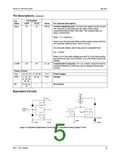
Pin Descriptions
Pin Number
Pin
Name
LQFP
PLCC
Value
Pin Function Description
Clock and Pixel I/O
CLK
26
27
TTL
Clock Input. The clock input is TTL-compatible and all pixel
data is registered on the rising edge of CLK. It is recommended
that CLK be driven by a dedicated TTL buffer to avoid reflection
induced jitter, overshoot, and undershoot.
R
47-40
9-2
23-16
6-1, 44-43
14-7
25-18
TTL
TTL
Red, Green, and Blue Pixel Inputs. The R, G, and B digital
inputs are TTL-compatible and registered on the rising edge of
CLK.
7-0
G
7-0
7-0
B
Controls
SYNC
11
16
Sync Pulse Input. Bringing SYNC LOW, turns off a 40 IRE
(7.62 mA) current source which forms a sync pulse on any D/A
converter output connected to IO . SYNC is registered on the
S
rising edge of CLK along with pixel data and has the same
pipeline latency as BLANK and pixel data. SYNC does not
override any other data and should be used only during the
blanking interval. If the system does not require sync pulses,
SYNC and IO should be connected to GND.
S
BLANK
WHITE
10
—
15
26
TTL
TTL
Blanking Input. When BLANK is LOW, pixel inputs are ignored
and the D/A converter outputs are driven to the blanking level.
BLANK is registered on the rising edge of CLK and has the
same two-pipe latency as SYNC and Data.
Force Full Scale Input. When WHITE is HIGH, pixel inputs are
ignored and the D/A converter outputs are driven to their full-
scale output level. A BLANK input overwrites a WHITE input.
WHITE is register on the rising edge of CLK and has the same
two-pipe latency as SYNC and Data.
SLEEP
—
28
TTL
Power-down Control Input. When HIGH, SLEEP places the D/
A converter in a low-power-dissipation mode. The D/A current
sources and the digital processing are disabled. The last data
loaded into the input and D/A registers is retained. This control is
asynchronous.
Video Outputs
IO
IO
IO
33
32
29
39
38
33
0.714 V
0.714 V
Red, Green, and Blue Data Outputs. The current source
outputs of the D/A converters are capable of driving RS-343A/
SMPTE-170M compatible levels into doubly-terminated 75 Ohm
lines. Sync pulses may be added to any D/A output.
R
G
B
p-p
IO
32
37
SYNC Current Output. When this pin is connected to any of the
D/A converter outputs, a 40 IRE offset is added to the video
level. When the SYNC input is LOW, the current is turned off,
bring the sync tip voltage to 0.0V. If no sync pulse is required,
S
p-p
(connected
to IO )
G
IO should be grounded. When SYNC is HIGH, the current
S
flowing out of IO is:
S
IO = 3.64 (V
REF
/ R )
REF
S
Voltage Reference
35
V
41
+1.235 V Voltage Reference Input/Output. An internal voltage source of
+1.235 Volts is output on this pin. An external +1.235 Volt
REF
reference may be applied here which overrides the internal
reference. Decoupling V
capacitor is required.
to GND with a 0.1µF ceramic
REF
4
REV. 1.02 11/24/99

 CADEKA [ CADEKA MICROCIRCUITS LLC. ]