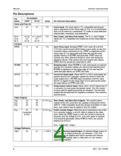
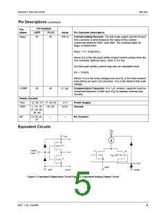
TMC3503
PRODUCT SPECIFICATION
Switching Characteristics
Parameter
Conditions2
Min
Typ1
10
1
Max
15
2
Units
ns
t
t
t
t
t
Clock to Output Delay
Output Skew
VDD = Min
D
ns
SKEW
R
Output Risetime
Output Falltime
10% to 90% of Full Scale
90% to 10% of Full Scale
to 3%/FS
2
3
ns
2
3
ns
F
Output Settling Time
15
ns
SET
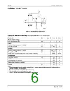
Notes:
1. Values shown in Typ column are typical for V
= +5V and T = 25°C.
A
DD
2. V
REF
= 1.235V, R
LOAD
= 37.5Ω, R
REF
= 590Ω.
System Performance Characteristics
Parameter
Conditions2
Min
Typ1
Max
Units
%/FS
%/FS
%
E
E
E
E
Integral Linearity Error
Differential Linearity Error
DAC to DAC Matching
Absolute Gain Error
Gain Error Tempco
V
V
V
V
V
V
, V
= Nom
= Nom
= Nom
= Nom
= Nom
±0.2
±0.2
3
±0.3
±0.3
10
LI
DD REF
, V
DD REF
LD
DM
G
, V
DD REF
, V
DD REF
TBD
%/FS
PPM/°C
nA
TC
EG
, V
DD REF
TBD
I
Output Off Current
= Max, R, G, B = 000h
DD
20
OFF
SYNC = BLANK = 0
PSRR Power Supply Rejection
Ratio
0.05
%/%
Notes:
1. Values shown in Typ column are typical for V
DD
= +5V and T = 25°C.
A
2. V
REF
= 1.235V, R
LOAD
= 37.5Ω, R = 590Ω.
REF
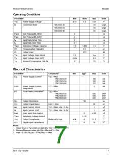
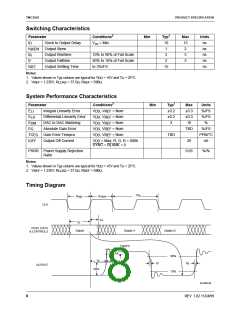
Timing Diagram
1/f
S
t
t
PWL
PWH
CLK
t
H
t
S
PIXEL DATA
& CONTROLS
DataN
DataN+1
DataN+2
3%/FS
90%
10%
t
D
t
SET
t
t
F
R
OUTPUT
50%
65-3503-04
8
REV. 1.02 11/24/99

 CADEKA [ CADEKA MICROCIRCUITS LLC. ]