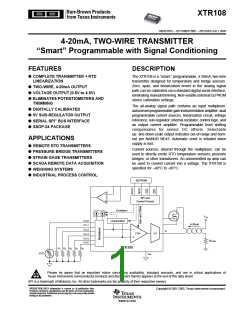
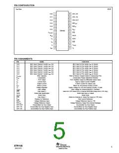
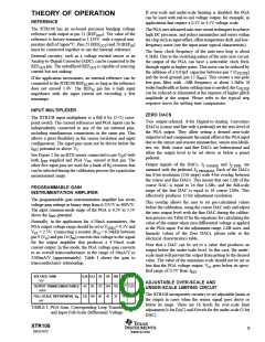
PIN CONFIGURATION
Top View
SSOP
V/I-0
V/I-1
V/I-2
V/I-3
V/I-4
V/I-5
CFILTER
RLIN
1
2
3
4
5
6
7
8
9
24 OPA +IN
23 OPA –IN
22 OPA OUT
21 REFOUT
20 REFIN
19 RSET
XTR108
18 CS1
17 SCLK
16 SDIO
15 CS2
VO
IIN 10
IO 11
14 VGATE
13 VS
IRET 12
PIN ASSIGNMENTS
PIN
NAME
FUNCTION
V/I-0
MUX Input Channel 0 and/or IREF Out
MUX Input Channel 1 and/or IREF Out
MUX Input Channel 2 and/or IREF Out
MUX Input Channel 3 and/or IREF Out
MUX Input Channel 4 and/or IREF Out
MUX Input Channel 5 and/or IREF Out
Filter Capacitor
MUX Input to PGA and/or IREF to Sensor
MUX Input to PGA and/or IREF to Sensor
MUX Input to PGA and/or IREF to Sensor
MUX Input to PGA and/or IREF to Sensor
MUX Input to PGA and/or IREF to Sensor
MUX Input to PGA and/or IREF to Sensor
Filter to Reduce Chopper Noise in Autozeroing PGA
Linearization Range Adjustment Resistor
PGA Amplified Output of Differential Sensor Input
Input to Output Current Amplifier
V/I-1
V/I-2
V/I-3
V/I-4
V/I-5
CFILTER
RLIN
Linearization
VO
PGA Output
IIN
Current Input
IO
Output Current
4-20mA Current for Output Loop
IRET
Return Current
Return for All External Circuitry Current
Supply Voltage for XTR and External Circuitry, If Used
Gate Voltage for External MOSFET Transistor
VS
Voltage Regulator
VGATE
CS2
Gate Voltage
Chip Select 2
Select for XTR Serial Port to External EEPROM (Output from XTR Only)
Serial Data Input or Output
SDIO
SCLK
CS1
Serial Data Input/Output
Serial Clock
Serial Clock
Chip Select 1
Select for External µC Serial Port (Input to XTR Only)
Sets Current Reference
RSET
Resistor for Reference
Voltage Reference Input
Voltage Reference Output
Uncommitted Op Amp Output
Uncommitted Op Amp Negative Input
Uncommitted Op Amp Positive Input
REFIN
REFOUT
OPA OUT
OPA –IN
OPA +IN
Voltage Reference Input to XTR
Voltage Reference Output from Internal Bandgap
Uncommitted Op Amp Output
Uncommitted Op Amp Negative Input
Uncommitted Op Amp Positive Input
XTR108
SBOS187C
5
www.ti.com

 BB [ BURR-BROWN CORPORATION ]