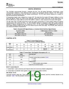
TSC2005
www.ti.com
SBAS379–DECEMBER 2006
OVERVIEW (continued)
Data Format
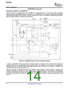
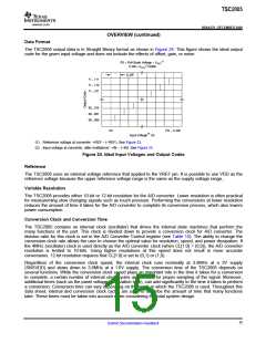
The TSC2005 output data is in Straight Binary format as shown in Figure 24. This figure shows the ideal output
code for the given input voltage and does not include the effects of offset, gain, or noise.
(1)
FS = Full-Scale Voltage = VREF
1LSB = VREF(1)/4096
1LSB
11...111
11...110
11...101
00...010
00...001
00...000
0V
FS - 1LSB
Input Voltage(2) (V)
(1) Reference voltage at converter: +REF – (–REF). See Figure 23.
(2) Input voltage at converter, after multiplexer: +IN – (–IN). See Figure 23.
Figure 24. Ideal Input Voltages and Output Codes
Reference
The TSC2005 uses an external voltage reference that applied to the VREF pin. It is possible to use VDD as the
reference voltage because the upper reference voltage range is the same as the supply voltage range, .
Variable Resolution
The TSC2005 provides either 10-bit or 12-bit resolution for the A/D converter. Lower resolution is often practical
for measureming slow changing signals such as touch pressure. Performing the conversions at lower resolution
reduces the amount of time it takes for the A/D converter to complete its conversion process, which also lowers
power consumption.
Conversion Clock and Conversion Time
The TSC2005 contains an internal clock (oscillator) that drives the internal state machines that perform the
many functions of the part. This clock is divided down to provide a conversion clock for A/D converter. The
division ratio for this clock is set in the A/D Converter Control register (see Table 15). The ability to change the
conversion clock rate allows the user to choose the optimal value for resolution, speed, and power dissipation. If
the 4MHz (oscillator) clock is used directly as the A/D converter clock (when CL[1:0] = (0,0)), the A/D converter
resolution is limited to 10-bits. Using higher resolutions at this speed does not result in more accurate
conversions. 12-bit resolution requires that CL[1:0] is set to (0,1) or (1,0).
Regardless of the conversion clock speed, the internal clock runs nominally at 3.8MHz at a 3V supply
(SNSVDD) and slows down to 3.6MHz at a 1.6V supply. The conversion time of the TSC2005 depends on
several functions. While the conversion clock speed plays an important role in the time it takes for a conversion
to complete, a certain number of internal clock cycles are needed for proper sampling of the signal. Moreover,
additional times (such as the panel voltage stabilization time), can add significantly to the time it takes to perform
a conversion. Conversion time can vary depending on the mode in which the TSC2005 is used. Throughout this
data sheet, internal and conversion clock cycles are used to describe the amount of time that many functions
take. These times must be taken into account when considering the total system design.
15
Submit Documentation Feedback

 BB [ BURR-BROWN CORPORATION ]