TSC2005
www.ti.com
SBAS379–DECEMBER 2006
OVERVIEW (continued)
ANALOG-TO-DIGITAL CONVERTER
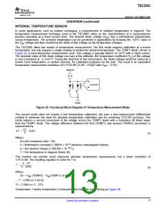
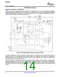
Figure 23 shows the analog inputs of the TSC2005. The analog inputs (X, Y, and Z touch panel coordinates,
chip temperature and auxiliary inputs) are provided via a multiplexer to the Successive Approximation Register
(SAR) Analog-to-Digital (A/D) converter. The A/D architecture is based on capacitive redistribution architecture,
which inherently includes a sample-and-hold function.
SNSVDD
VREF
PINTDAV
SNSVDD
Level Shift
RIRQ
51kW
Preprocessing
Data
Pen Touch
Available
Zone
Control
Logic
Detect
MAV
C3-C0
AGND
X+
X-
SNSVDD
Y+
+REF
+IN
Y-
Converter
-IN
-REF
SNSGND
AUX
AGND
Figure 23. Simplified Diagram of the Analog Input Section
A unique configuration of low on-resistance switches allows an unselected A/D converter input channel to
provide power and an accompanying pin to provide ground for driving the touch panel. By maintaining a
differential input to the converter and a differential reference input architecture, it is possible to negate errors
caused by the driver switch on-resistances.
The A/D converter is controlled by two A/D Converter Control registers. Several modes of operation are
possible, depending on the bits set in the control registers. Channel selection, scan operation, preprocessing,
resolution, and conversion rate may all be programmed through these registers. These modes are outlined in
the sections that follow for each type of analog input. The conversion results are stored in the appropriate result
register.
14
Submit Documentation Feedback

 BB [ BURR-BROWN CORPORATION ]