PCM3793A
PCM3794A
www.ti.com
SLAS529A–JANUARY 2007–REVISED FEBRUARY 2007
THREE-WIRE INTERFACE (SPI, MODE (PIN 28) = LOW)
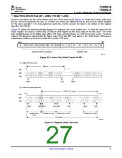
All write operations for the serial control port use 16-bit data words. Figure 30 shows the control data word
format. The most-significant bit must be 0. There are seven bits, labeled IDX[6:0], that set the register address
for the write operation. The least-significant eight bits, D[7:0], contain the data to be written to the register
specified by IDX[6:0].
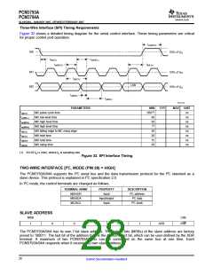
Figure 31 shows the functional timing diagram for writing to the serial control port. To write the data into the
mode register, the data is clocked into an internal shift register on the rising edge of the MC clock. The serial
data should change on the falling edge of the MC clock, and MS should be LOW during write mode. The rising
edge of MS should be aligned with the falling edge of the last MC clock pulse in the 16-bit frame. MC can run
continuously between transactions while MS is in the LOW state.
LSB
D0
MSB
0
IDX6 IDX5 IDX4 IDX3 IDX2 IDX1 IDX0
Register Index (or Address)
D7
D6
D5
D4
D3
D2
D1
Register Data
R0001-01
Figure 30. Control Data Word Format for MD
(1) Single Write Operation
16 Bits
MS
MC
MD
MSB
LSB
MSB
(2) Continuous Write Operation
8 Bits x N Frames
MS
MC
MD
MSB
LSB MSB
LSB MSB
LSB
MSB
LSB
Register Index
8 Bits
Register (N) Data
Register (N+1) Data
N Frames
Register (N+2) Data
T0012-03
Figure 31. Register Write Operation
27
Submit Documentation Feedback

 BB [ BURR-BROWN CORPORATION ]