PCM3793A
PCM3794A
www.ti.com
SLAS529A–JANUARY 2007–REVISED FEBRUARY 2007
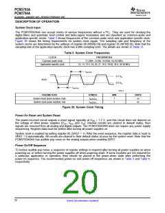
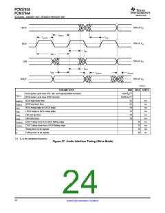
50% of VIO
LRCK
tw(BCL)
tw(BCH)
t(LB)
50% of VIO
50% of VIO
50% of VIO
BCK
t(BL)
t(BCY)
DIN
t(DH)
t(DS)
t(CKDO)
t(LRDO)
DOUT
T0010-09
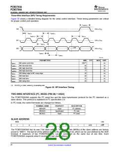
PARAMETERS
MIN
MAX UNITS
BCK pulse cycle time (I2S, left- and right-justified formats)
BCK pulse cycle time (DSP format)
BCK high-level time
1/(64 fS)(1)
1/(256 fS)(1)
t(BCY)
tw(BCH)
tw(BCL)
t(BL)
35
35
10
10
10
10
ns
ns
ns
ns
ns
ns
BCK low-level time
BCK rising edge to LRCK edge
LRCK edge to BCK rising edge
DIN set up time
t(LB)
t(DS)
t(DH)
DIN hold time
t(CKDO) DOUT delay time from BCK falling edge
15
15
10
10
ns
ns
ns
ns
t(LRDO)
DOUT delay time from LRCK falling edge
Rising time of all signals
tr
tf
Falling time of all signals
(1) fS is the sampling frequency.
Figure 27. Audio Interface Timing (Slave Mode)
24
Submit Documentation Feedback

 BB [ BURR-BROWN CORPORATION ]