PCM3793A
PCM3794A
www.ti.com
SLAS529A–JANUARY 2007–REVISED FEBRUARY 2007
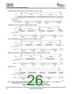
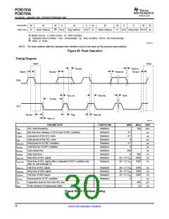
Transmitter
Data Type
M
M
M
S
M
S
M
M
M
S
S
M
M
NACK
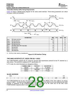
St
Slave Address
W
ACK
Reg Address
ACK Sr
Slave Address
R
ACK Read Data
Sp
M: Master Device S: Slave Device St: Start Condition
Sr: Repeated Start Condition ACK: Acknowledge Sp: Stop Condition NACK: Not Acknowledge
W: Write R: Read
R0002-02
NOTE: The slave address after the repeated start condition must be the same as the previous slave address.
Figure 35. Read Operation
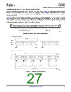
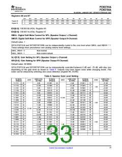
Timing Diagram
Start
Stop
t
t
(SDA-F)
(D-HD)
t
t
t
t
(P-SU)
(BUF)
(D-SU)
(SDA-R)
SDA
t
t
t
(SP)
(SCL-R)
(RS-HD)
t
(LOW)
SCL
t
t
t
(RS-SU)
(S-HD)
(HI)
t
(SCL-F)
T0050-03
PARAMETERS
SCL clock frequency
CONDITIONS
MIN
MAX
UNIT
fSCL
Standard
Standard
Standard
Standard
Standard
Standard
Standard
Standard
Standard
Standard
100
kHz
µs
µs
µs
µs
µs
ns
ns
ns
ns
t(BUF)
Bus free time between a STOP and START condition
Low period of the SCL clock
High period of the SCL clock
Setup time for START condition
Hold time for START condition
Data setup time
4.7
4.7
4
t(LOW)
t(HI)
t(RS-SU)
t(S-HD)
t(D-SU)
t(D-HD)
t(SCL-R)
t(SCL-R1)
4.7
4
250
0
Data hold time
900
1000
1000
Rise time of SCL signal
20 + 0.1 CB
20 + 0.1 CB
Rise time of SCL signal after a repeated START condition and
after an acknowledge bit
t(SCL-F)
t(SDA-R)
t(SDA-F)
t(P-SU)
CB
Fall time of SCL signal
Standard
Standard
Standard
Standard
20 + 0.1 CB
20 + 0.1 CB
20 + 0.1 CB
4
1000
1000
1000
ns
ns
ns
µs
pF
ns
Rise time of SDA signal
Fall time of SDA signal
Setup time for STOP condition
Capacitive load for SDA and SCL line
Pulse duration of suppressed spike
400
25
t(SP)
Figure 36. I2C Interface Timing
30
Submit Documentation Feedback

 BB [ BURR-BROWN CORPORATION ]