PCM3793A
PCM3794A
www.ti.com
SLAS529A–JANUARY 2007–REVISED FEBRUARY 2007
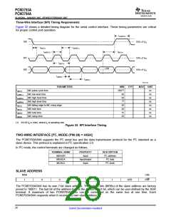
Three-Wire Interface (SPI) Timing Requirements
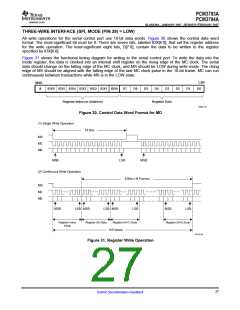
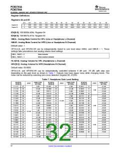
Figure 32 shows a detailed timing diagram for the serial control interface. These timing parameters are critical
for proper control port operation.
t
w(MHH)
MS
50% of V
IO
t
t
w(MCL)
(MLS)
t
t
(MLH)
w(MCH)
MC
MD
50% of V
IO
t
(MCY)
LSB
50% of V
IO
t
(MDS)
t
(MDH)
T0013-08
PARAMETERS
MIN
TYP
MAX
UNIT
t(MCY)
tw(MCL)
tw(MCH)
tw(MHH)
t(MLS)
MC pulse cycle time
MC low level time
MC high level time
MS high level time
500(1)
ns
ns
ns
ns
ns
ns
ns
ns
50
50
(1)
MS falling edge to MC rising edge
MS hold time
20
20
15
20
t(MLH)
t(MDH)
t(MDS)
MD hold time
MD setup time
(1) 3/(128 fS) s (min), where fS is sampling rate.
Figure 32. SPI Interface Timing
TWO-WIRE INTERFACE [I2C, MODE (PIN 28) = HIGH]
The PCM3793A/94A supports the I2C serial bus and the data transmission protocol for the I2C standard as a
slave device. This protocol is explained in I2C specification 2.0.
In I2C mode, the control terminals are changed as follows.
TERMINAL NAME
MS/ADR
PROPERTY
Input
DESCRIPTION
I2C address
I2C data
MD/SDA
Input/output
Input
MC/SCL
I2C clock
SLAVE ADDRESS
MSB
LSB
R/W
1
0
0
0
1
1
ADR
The PCM3793A/94A has its own 7-bit slave address. The first six bits (MSBs) of the slave address are factory
preset to 100011. The last bit of the address byte is the device select bit, which can be user-defined by the ADR
terminal. A maximum of two PCM3793A/94As can be connected on the same bus at one time. Each
PCM3793A/94A responds when it receives its own slave address.
28
Submit Documentation Feedback

 BB [ BURR-BROWN CORPORATION ]