ꢀ ꢁꢂ ꢃ ꢄ ꢅ ꢆ
www.ti.com
SLES100 − DECEMBER 2003
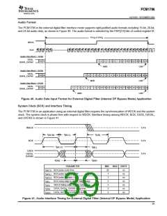
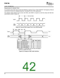
Requirements for System Clock
For operation in the DSD mode, the bit clock (DBCK) is required on pin 7 of the PCM1796. The frequency of the bit
clock can be N times the sampling frequency. Generally, N is 64 in DSD applications.
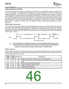
The interface timing between the bit clock and DSDL and DSDR is required to meet the setup and hold time
specifications shown in Figure 44.
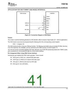
t = 1/(64 ×44.1 kHz)
DBCK
DSDL
DSDR
D0
D1
D2
D3
D4
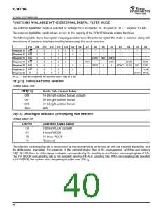
Figure 43. Normal Data Output Form From DSD Decoder
t
t
(BCL)
(BCH)
1.4 V
1.4 V
DBCK
t
(BCY)
DSDL
DSDR
t
t
(DH)
(DS)
PARAMETER
MIN MAX UNITS
(1)
t
DBCK pulse cycle time
DBCK high-level time
DBCK low-level time
85
ns
ns
ns
ns
ns
(BCY)
t
30
30
10
10
(BCH)
t
(BCL)
(DS)
(DH)
t
t
DSDL, DSDR setup time
DSDL, DSDR hold time
(1)
2.8224 MHz × 4. (2.8224 MHz = 64 × 44.1 kHz. This value is
specified as a sampling rate of DSD.)
Figure 44. Timing for DSD Audio Interface
42

 BB [ BURR-BROWN CORPORATION ]