PCM1753
PCM1754
PCM1755
www.ti.com
SLES092A – OCTOBER 2003 – REVISED AUGUST 2004
ZREV: Zero Flag Polarity Select
Default value: 01h
ZREV = 0
ZREV = 1
High on zero flag pins indicates a zero detect (default)
Low on zero flag pins indicates a zero detect
The ZREV bit allows the user to select the polarity of zero flag pins.
AZRO: Zero Flag Function Select
Default value: 0
AZRO = 0
AZRO = 1
L-/R-channel independent zero flags (default)
L-/R-channel common zero flag
The AZRO bit allows the user to select the function of zero flag pins.
AZRO = 0:
Pin 11: ZEROR, zero flag output for R-channel
Pin 12: ZEROL, zero flag output for L-channel
Pin 11: ZEROA, zero flag output for L-/R-channels
Pin 12: NA, not assigned
AZRO = 1:
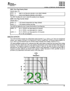
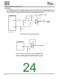
ANALOG OUTPUTS
The PCM1753/54/55 includes two independent output channels, V
L and V
OUT
R. These are unbalanced
OUT
outputs, each capable of driving 4 V p-p typical into a 5-kΩ ac-coupled load. The internal output amplifiers for
L and V R are biased to the dc common-mode (or bipolar zero) voltage, equal to 0.5 V
V
.
CC
OUT
OUT
The output amplifiers include an RC continuous-time filter, which helps to reduce the out-of-band noise energy
present at the DAC outputs due to the noise shaping characteristics of the PCM1753/54/55 delta-sigma D/A
converters. The frequency response of this filter is shown in Figure 26. By itself, this filter is not enough to
attenuate the out-of-band noise to an acceptable level for many applications. An external low-pass filter is
required to provide sufficient out-of-band noise rejection. Further discussion of DAC post-filter circuits is
provided in the Applications Information section of this data sheet.
LEVEL
vs
FREQUENCY
10
0
−10
−20
−30
−40
−50
−60
0.1
1
10
100
1k
10k
f – Frequency – kHz
Figure 26. Output Filter Frequency Response
23

 BB [ BURR-BROWN CORPORATION ]